Because of the holidays, TI E2E™ design support forum responses will be delayed from Dec. 25 through Jan. 2. Thank you for your patience.

This thread has been locked.

If you have a related question, please click the "Ask a related question" button in the top right corner. The newly created question will be automatically linked to this question.

LF198-N: Null offset on Output at power up

Part Number: LF198-N

Tool/software:

Dear Technical Supporters,

Hope you are doing well.

I'd like to get some information about Null offset of LFx98 on Output Line during power up.

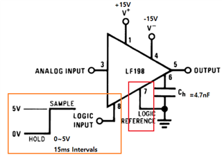
In my schematic, it was designed with ±15V power supply and same as below.
I'd like to get 0V voltage on output when power up, but there were about 400mV on the output although there was 0V on Analog Input.
(There are 4 channels in my design and they have outputs as about 400mV as.)

I already checked Logic Input but there was nothing signal logic high during power up.

Q1. If there are a few difference with ±15V Supply voltage, would it affect output offset voltage?

Q2. If not, are there something factors that make offset on output line?

  • Hi Kim,

    Q1. If there are a few difference with ±15V Supply voltage, would it affect output offset voltage?

    Q2. If not, are there something factors that make offset on output line?

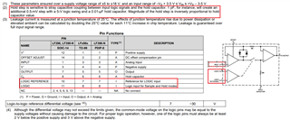
    Below is the logic reference and logic input requirements. Upon power up, there may be voltage spikes that cause Logic input to be triggered. What is voltage of the Logic Reference? It is connected to GND, then the comparator may be triggered during the power up, and  initiated unwanted charge up in the Ch holding capacitor (sample and hold events). I do not have your actual schematic, and this is just my speculation currently.  

    Could you provide me more detailed information and schematic about the circuit? Maybe I am able to figure it out what is going on. 

    If you have other questions, please let me know.

    Best,

    Raymond

  • Dear Raymond,

    Thank you for your fast reply.

    I wish I could you give more detail schematic, but I couldn't.

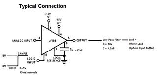
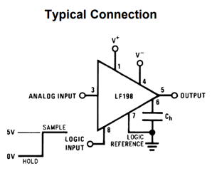
    Instead, I'll give you more detail symbol of my schematic.

    Please see below.

    Capacitors(Charging, Low Pass Filter) are all C0G(5% Tolerance) MLCC Type Capacitors.

    Q1. Could you let me know the maximum offset output during power up?

    Q2. Is there any method to reduce offset output?

    Thank you in advance.

    Best Regards,

    Wantae, Kim

  • Hi Wantae,

    Without the schematic, it will be tough to troubleshoot. I can only make some educated guess. 

    1. Please tie to Analog input or pin3 to GND, when dual rails are powered up (I do not know if there is an input option to do that). At least you can check out if the input analog is related to the issues.

    2. Place a known reference voltage at pin7 (instead of tied to GND). The sample and hold logic input is referenced to Pin7. If there is voltage or current transient event during power up, it has to exceed the input logic voltage in order to perform the function.  

    3. Discharge Ch or pin6 should remove the hold voltage at the output or pin5 (you can measure the voltage at pin6, and check it out before and after the powerup sequences). 

    These are my suggestions for now. Please let me know if this is able to resolver your issues. 

    Best,

    Raymond