Because of the Thanksgiving holiday in the U.S., TI E2E™ design support forum responses may be delayed from November 25 through December 2. Thank you for your patience.

This thread has been locked.

If you have a related question, please click the "Ask a related question" button in the top right corner. The newly created question will be automatically linked to this question.

OPA828: Simulating a supply-bootstrapped amplifier circuit in TINA

Part Number: OPA828
Other Parts Discussed in Thread: OPA827, OPA810, OPA1656, UA741, OPA596, OPA593, LM4040, OPA197, OPA192

Tool/software:

Dear Support Team,

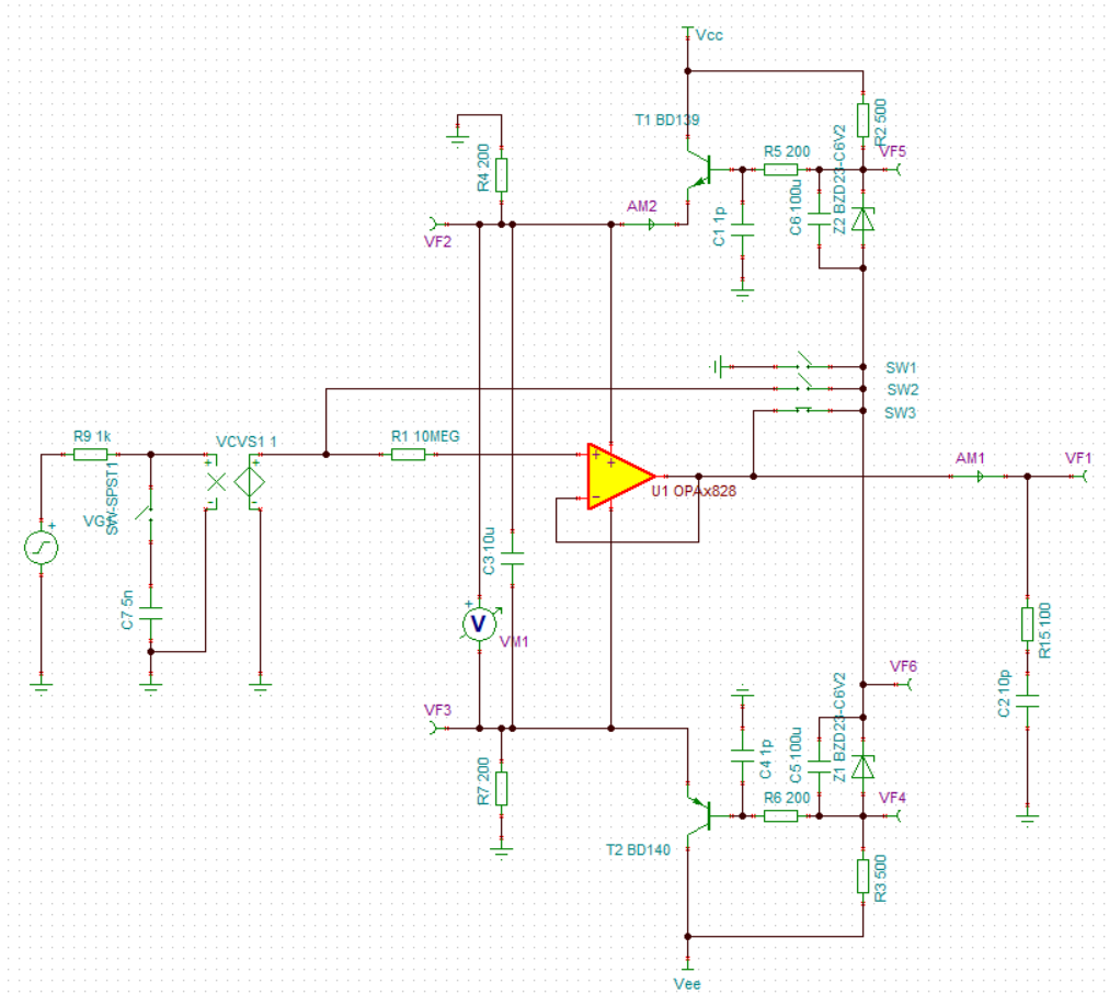
We are trying to verify the behavior of a supply-bootstrapped circuit using OPA828 in a TINA simulations. The purpose of the circuit is to reduce the common mode input impedance.

 IN_BOOTSTR_OPA828_1a.TSC

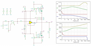
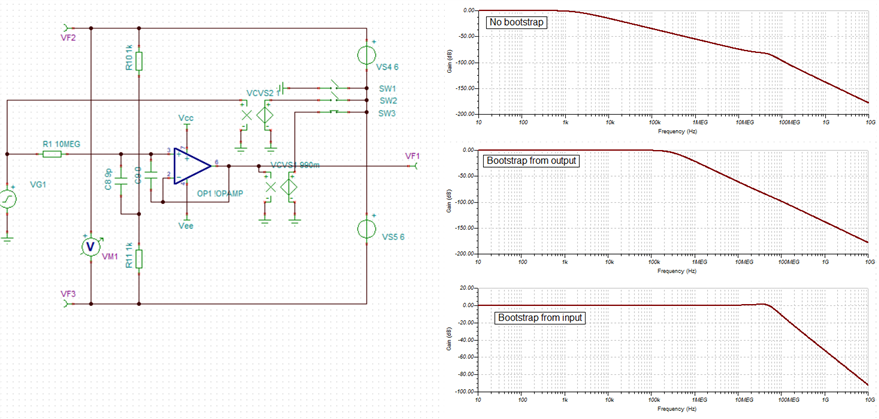
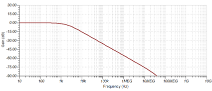
However, we can see no difference between SW1 short and SW3 short (bootstrap off vs. bootstrap from output) -- the bandwidth reamains unchanged as in the two graphs below.
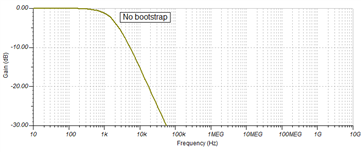
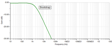
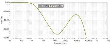
We can also observe strange effects with SW2 short (bootstrap from input):
We have also tried OPA810, OPA827, OPA1656 with no better results.

Interestingly, when OPA828 is replaced with the venerable uA741, the simulation shows noticeable increase in bandwidth as one could expect.

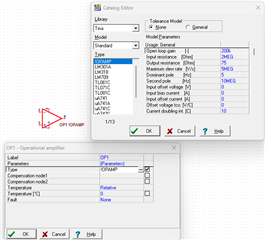
The OPA828 model includes the input capacitance (parameter named "Zic"), what can be the reason we cannot see any improvement in the frequency characteristics due to the bootstrap for OPA828 while uA741 behaves as expected? Is that a problem of the model, or should we expect such results in reality?

Best regards,

Michal

  • Hi Michal,

    We are trying to verify the behavior of a supply-bootstrapped circuit using OPA828 in a TINA simulations.

    The op amp bootstrapped technique is typically implemented in operating at high voltage of a given op amp. OPA828 is ±18Vdc dual supply op amp, and I would recommend OPA596 or OPA593 is you want to increase the voltage supply rails. We have many other op amp that can handle higher voltage supply rails. 

    https://www.ti.com/lit/an/sboa510/sboa510.pdf?ts=1723565234011&ref_url=https%253A%252F%252Fwww.ti.com%252Fproduct%252FOPA462%253Fbm-verify%253DAAQAAAAJ_____1oaogoE_6TjItY-6DozbBgHQnoZGToK0Ks8PcSv9wMMbwAMjlVIOWzCQ5oGZdYhLyAuWOu7go1Wq-k2ZxilhpuzgCnmnmUBKcUT7k09rJdIN_Sjr3z3fq0HOg0j3CZTuvmPru-W4MlCGeP3kuaXhRcOtsEkTealrPzAFx13y0IBYZAVxjMPQCAGaZ81EEE-xur5kbdtBu6fB9lvJJz7mtVaHR37NVXObzFTTPyP0ytAAFbvaMMDvUykELPUq1xkwJbtLuu1EnnYySoGAzvb85xh_6tJWdbcBGM9SGzG9z8b

    The purpose of the circuit is to reduce the common mode input impedance.

    I do not understand the purpose of the design approach. Normally, you want to have the common mode input impedance as high as possible to reduce the input loading effects. Could you explain?

    FYI. An op amp's input impedance is a function of the loop gain. If you reduce the loop gain, you would reduce the input impedance. 

    In the enclosed sboa510 application note, you may use lower cost op amps to boost the OPA828's supply rail. The the discrete bootstrapped approach will work, but part counts are high and it is difficult to troubleshoot. I would use some lower cost op amp, such as our General Purpose op amps that have the current rating to drive the rails of OPA828. Or you may use OPA596/OPA593 to drive your intended application. 

    Please let me know what you are trying to do and I may be able to provide you with other suggestions. 

    Best,

    Raymond

  • Hi Raymond,

    Our mistake - one word was missing. The purpose is to reduce the common mode input CAPACITANCE. We need to achieve both low input offset voltage, high input resistance, low bias current and wide frequency response for high impedance sources.  OPA828 has a good offset voltage, but its input common mode capacitance of 9 pF is large and limits our frequency response very much. 

    What's important is how the opa828's common mode capacitance has been accounted in the amplifier TINA model.  

    The solution from the sboa510 using two additional amplifiers is unnecessarily complicated at this stage. We prefer the approach as in Figure 4-2 in the same document. 

    Loop gain affects mainly differential impedance, harder to affect common mode impedance....

    All the simulation results of the circuit we presented are correct (behavior of bootstrap circuit with transistors), except for the lack of change in frequency response. We have some suspicions about this and are already able to modify the simulation circuit so that the bootstrap effect on the frequency response simulation results begin to look correct, but we prefer to wait for your analysis.

    Best regards,

    Marcin (In place of Michal, who is temporarily absent)

  • Hi Marcin,

    OPA828 has a good offset voltage, but its input common mode capacitance of 9 pF is large

    Is there a reason you place 10MΩ at the non-inverting input, where the common mode capacitance is 9pF? In the bottom simulation, I changed 10MΩ to zero and increase the bandwidth of the op amp. OPA828 has the unity gain bandwidth at approx. 45MHz (GBP). 

    BTW, I meant to say the input common mode impedance is Zin*Aol. 

    If you have other questions, please let me know. 

    Best,

    Raymond

  • Hi Raymond,

    The signal source in our case may have a very high impedance. Possibly even on the order of several MOhm. That is why there is a 10MOhm resistor in the simulation.
    The problem is to get a combination of the characteristics we wrote about above - high input impedance, low offset and wide bandwidth (~100 kHz). The answer could be to use power supply bootstrapping, but in simulations for most operational amplifier models this completely fails.

    Let me emphasize again - our question is why opa828, opa827, opa810 (...) models do not show in simulations the effect of removing input common capacitance after applying power supply bootstrapping. We suspect a significant bug in the amplifier models.

    Best regards,

    Marcin.

  • Hi Marcin, 

    We suspect a significant bug in the amplifier models

    There is no significant bug in our Spice model regarding to the common and differential mode capacitance. 

    In our Precision Op Amp Spice model, the common and differential input capacitance are modeled, see the link below. If you open OPA828's macro file, you will find these defined digures.   

     uA741 Spice model is likely not modeled at the input common and differential capacitance. It you are using the following ideal op amp model from Tina or other simulator, the input common and differential capacitance figures are not modeled. this is the likely the reason that you see the bandwidth increase, because the input signal is not going through LPF, where the input 10MΩ interacts with 9pF at the input) 

    If your application has very high input impedance, I would suggest to use our HS Op amp as buffer, where it has much lower common and differential mode capacitance. Once it is buffered, you can connect it to OPA828, if you prefer the op amp. 

    Alternatively, you may take our input device, such as mosfet, FET input stage and convert the high input impedance signal to low output impedance. 

    In PRAMPS product, our op amp products' BW is limited up to 50MHz, and OPA828 is listed toward the high side of bandwidth products. In HS op amp product, some of the common mode input capacitance is only a few pF, because their products are required to support up to > 100s GHz bandwidth, see the link below. 

    https://www.ti.com/amplifier-circuit/op-amps/high-speed/products.html#sort=512;desc&

    Anyway, if you have other questions, please let me know. 

    Best,

    Raymond


  • Hi Raymond,

    Thank you for your notes. Obviously, we do not know the inner details of the models, but we guess that some elements of the uA741 model cause, even if not directly, the effect of varying (bootstrapped) supply on the frequency characteristics.

    The use of a buffer amplifier is not desirable in our application because it would add some offset which we are trying to avoid by using a low-offset amplifier as OPA828.

    We suspect that the problem with the model may be that it is not designed for floating supply conditions and it has not been tested well in such circumstances. This is why we would like to know how the common mode capacitance is modeled.

    The assumption that all models are free of errors is too idealistic, we are afraid. Take this example -- a simple shunt 5 V voltage reference: The three schematics above are identical except of the point of ground connection. None of the voltages calculated in the simulation are ground-referenced so why are they different? There should be 5 V between the terminals of every LM4040, but only the top LM4040 in the leftmost schematics behaves as expected. (Interestingly, LM4040_C25 model does not exhibit this problem, there is 2.5 V on each one.) It looks like there is a direct reference to system ground potential somewhere in the model (some hidded third terminal to GND) which causes that the model only works correctly in typical applications with anode at GND.
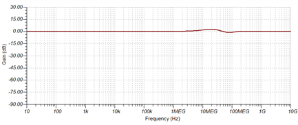
    We suspect a similar problem in the model of OPA282 (and many other amplifier). Please have a look at this simple circuit -- an amplifier with split-supply:

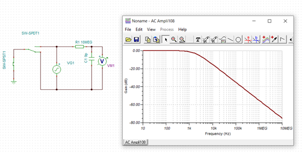
    The results surprisingly depend on where the ground is connected (SW-SPDT1 switch):

    The simulation results should not depend on the point of ground connection, but the difference above is drastical. It suggests that there is some hidden reference to the ground potential in the model. If so, it could also influence the model of the input common mode impedance. It might not be an error, just a simplification which may work well in a typical case of fixed supply voltages and fail with any kind of floating supplies.

    (Side note: uA741, TL71 and a few other amplifiers which have their models built into TINA do not exhibit the above behavior.)

    The best solution would be to review and slighly modify the model. If it is not possible in short perspective, we would like to know at least where to put the ground reference in our model circuit to achieve the most realistic behavior and simulation results.

    Best regards,

    Michal

  • Hi Michal,

    I am unable to reproduce the plot you presented on the left. Where did you get AC response of 10G from? 

    Yes, op amp does not require GND reference in order to work, but it needs to have a reference. OPA828's GBP is approx. 45 MHz.  

    OPA828 w 10Mohm R 08142024.TSC

    Best,

    Raymond

  • Hi Raymond,

    Your example uses voltage pin named Vout, which shows voltage with respect to ground, but your schematic has no explicitly defined ground. Is this documented anywhere what a voltage pin shows in such a case? When we replace the voltage pin with a voltage meter referenced to mid-supply, the results are as in our simulation.

    IN_BOOTSTR_OPA828_1b4_reduced2.TSC

    In a simple circuit below (RC filter corresponding to input capacitance of OPA828), the results do not change if we switch the ground between the top and the bottom of VG1, or if we disconnect ground at all. The characteristic frequncy is ca. 1 kHz.

    RC_In_opa828.TSC

    In your schematics with no GND connection it was ca. 1 kHz with a voltage pin and ca. 100 kHz with a voltmeter. The voltmeter results should be more reliable as it is precisely defined between which points they are measured. Comparing the results of the simple RC filter with OPA828 simulations, we get:

    1. GND connected to the negative terminal of VG1 driving OPA828 -- the results are correct (same as for the RC filter);

    2. GND connected to the positive terminal of VG1 driving OPA828 -- the results are much different from RC filter, so thay cannot be correct;

    3. GND not connected anywhere -- the results are yet different, so thay cannot be correct either.

    Summarizing, the simulation results depend on where the GND connection is, which cannot be explained in other way than that there is some hidden reference to GND in the amplifier model.

    Best regards,

    Michal

  • Hi Michal,

    I have trying to provide you the hint that 10MΩ and common mode capacitance 9pF will generate the pole that determines the bandwidth of the op amp (e.g. OPA828). The dominated pole is occurred at 1.77 kHz as simulated from the get-go.

    In bootstrapped op amp configuration, the boosted supply rails are synchronized and delta voltage at any given time can not exceed the max. operating voltage of an op amp. For OPA828, this is 36Vdc. Your configuration is not closed to this delta voltage (~24Vdc), but I do not see how you are able to extend the bandwidth OPA828, if the input signal has pole close to 1.77 kHz.  

    The following technique may help if you have large input impedance, say 10MΩ:

    1. buff the input signal (use HS op amp with input common mode capacitance in 1-2pF). Some ultra HS op amp may go down to ~0.5pF in Ccm. 

    2. Use voltage divider and amplifier the signal afterwards, say use OPA828, difference amplifier or instrumentation amplifier. 

    3. Have you try to AC couple your input signal, say up to 0.1uF to 1uF capacitor instead? This will extend your bandwidth of OPA828

    4. There may be a way to introduce a parasitic capacitance between the inverting and noninverting input to lower the common mode capacitance effect in OPA828. 

    Anyway, these are on top my head currently. If you tell me what frequency range you are trying to operate, maybe I can provide you with additional suggestion. 

    Best,

    Raymond

  • Hi Raymond,

    We are perfectly aware of the low-pass filter that forms at the input of the amplifier. It is not important to know whether it is 1.77 kHz or less, the important thing is that under NORMAL conditions it actually limits the bandwidth of the entire system. We must have a bandwidth at least an order higher.
    And, again, let me clarify that we cannot use an additional buffer, because it will INTRODUCE an unacceptably large offset error! In such situations, more advanced methods of bandwidth expansion are usually used. The best known is the positive feedback technique, where a correction current is “injected” into the input of the amplifier through an experimentally selected small capacitor using just positive feedback. We have used it successfully before, and we know that it has significant drawbacks - it unfortunately requires for full effectiveness “tuning” individually for given input conditions (source impedance). If the source impedance changes, the method can lead to instability or weaker performance. This method is somewhat similar (only much stronger) to the increase in capacitance between the inputs of the amplifier you proposed.
    The second, somewhat less commonly used, because apparently more complicated, is precisely bootstrapping the input buffer supply, which is what we are trying to simulate. Attached is a sample scientific publication that proves that power supply bootstrapping can virtually reduce the amplifier's common input capacitance by up to several orders. Supply bootstrapping works similarly to active/driven shielding.

    Ultra-high_input_impedance_buffer_for_dry_or_capacitive_electrodes_Design_and_characterization_for_industry.pdf

    Back to the point.
    1. We don't need help here in analyzing how the power supply bootstrapping method works on the apparent input capacitance of the amplifier, because we know how it works and have seen it in action.
    2. We don't need help in selecting input buffers, because we have carefully analyzed all of them ourselves for several weeks!
    3. Instead, we need an explanation of why a phenomenon occurring in real systems (laboratory) cannot be simulated in TINA - why bootstrapping has no effect on bandwidth in the case of large source impedance.

    As we have clearly shown with the example of the LM4050, errors in circuit models are common - people really make mistakes and this should be accepted.

    We have clearly shown that, using the opa828 model, we are dealing with phenomena, which cannot be explained in any other way than by the limitations of its model.

    We are almost certain that the problem of the inability to simulate correctly bootstrapping is related to some simplifications/limitations of the consideration of the input common capacitance. Therefore, we need information from someone familiar with these models on how the common capacitance modeling was done. With this information, we will be able to consciously create such a circuit in TINA that simulates correctly.

    We also don't need any additional suggestions, because this is not the first system of this type that we have created - others have been working on production lines for many years and we know what we need and what we have. We only need information on how the common capacitance was taken into account in the models of your amplifiers, so that we can make our lives easier and use simulation before creating a prototype.

    Best Regards,

    Marcin.

  • Hi Marcin,

    Supply bootstrapping works similarly to active/driven shielding.

    I am aware of the two techniques. I do know that the bootstrapping in op amp topology will increase apparent input impedance. However, I am not aware that the bootstrapping technique has much impact on reducing the input common mode capacitance in buffer configuration. Anyway, I have asked my colleague to take a look your query, perhaps he has some ideas about this approach or Spice model. 

    For ionic electrochemical interface showed in the image below is nothing new, and it will take advantage of the bandwidth of the OPA828... 

    If you have other questions, please let us know. 

    Best,

    Raymond

  • Marcin,

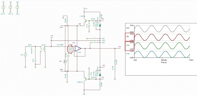
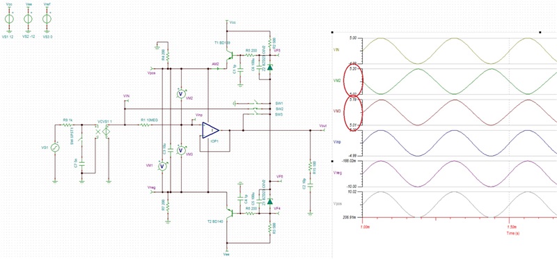
    Let me first say that in order for your bootstrap circuit to work properly, you would need to have the supplies following VIN and not Vinp nor Vout (see below) and therefore SW2 would need to be closed and NOT SW1 nor SW3. Using your circuit together with an ideal op amp (where Cin_cm =0) shows no attenuation at Vinp and Vout.as you would expect.

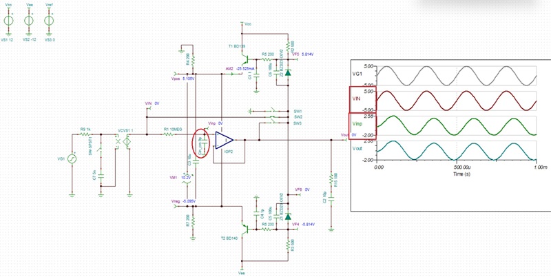
    However, as you correctly pointed out despite bootstrapping of the supplies there is Cin_cm effect at work here that attenuates the signal at Vinp - see below.

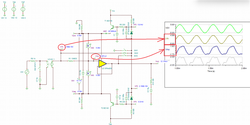
    Using actual model of OPA828 shows also significant distortion - see below.

    Some of the effect comes from the fact that your bootstrapping circuit has some variation of VM2 and VM3 (see below) that ideally should be fixed exactly at 5V. 

    However, the main reason for the bootstrapping not working as you would expect is the fact that in order for any macro-model to work all internal nodes must be referenced to a system ground whereas the actual IC circuits do not have fixed internal ground. For this reason, all internal nodes are referenced to the floating ground (MID), which is set in the middle of the supply voltages. However, in order to desensitize the modulation of internal nodes by variation of the supply voltage, the floating ground has a low-pas filter - this causes a delayed response (phase shift) and is behind the problem you see. The delay response of internal ground modulates the voltage across Cin_cm and results in the signal attenuation you see.  All in all, macro-models have their limitations as shown in the case of bootstrapped supplies that prevents elimination or reduction of Cin_cm effect on the simulated bandwidth. 

  • Hi Marek,

    Indeed, using the input signal for bootstrapping gives the best possible effect. However, one can get quite much bandwidth improvement using the output signal. The universal amplifier inserted into the circuit below simulates OPA828 by setting its parameters (open loop gain, output resistance etc.) and adding CM input capacitance (C8) in the proper way, i.e., to mid-supply instead of GND. As it can be seen from the results below, using the input signal gives maximum bandwidth, but with the output signal there is still 100x bandwidth improvement which is often sufficient.

    The second of your circuits, as we understand, is an example of how the Cin_cm connected to GND does not react to the bootstrapping effect. This is why we were afraid the CM capacitance in the model was internally connected to GND and prevented correct simulation of bootstrapping.

    The distortion in the third picture is something that we have already seen in our previous simulations. The changes of the input signal are delayed with respect to the changes of the supply voltages due to the input capacitance, and in effect the input voltage exceeds the momentary acceptable common mode input range.

    Finally, thank you for revealing the details of the inner working of the model. The existence of the low-pass filter on the internal reference level explains the difficulties in simulating the bootstrapping. However, even with the low-pass filter, there should be seen some small effect of bootstrapping, and there is none. Second, this does not explain at all the strange behavior of the model observed when the point of the GND connection was changed in the circuit. That still suggests some issue related to GND level in the model.

    Would it be possible to get a model of OPA828 without Cin_cm to avoid the low-pass filter effect? The Cin_cm could be then simulated with an external capacitor connected to unfiltered mid-supply as in the picture above.

    Regards,

    Michal

  • Hi Michal,

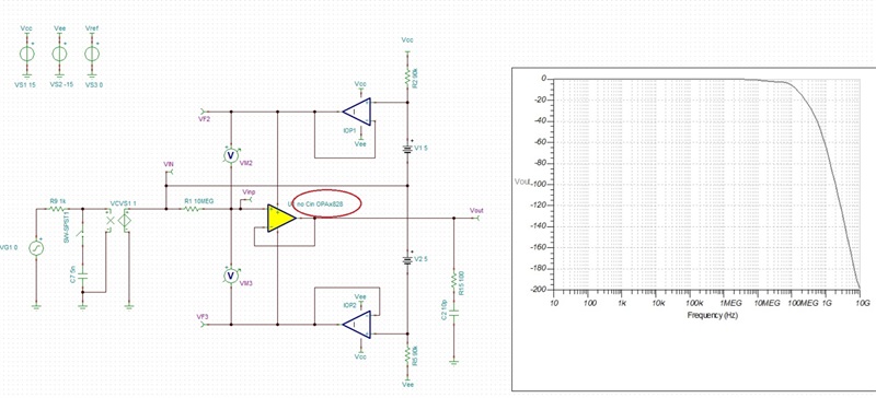
    Attached please find the OPA828 macro-model you requested with removed Cin capacitance.  As you would expect, it extends the bandwidth of the bootstrapped application - see below. 

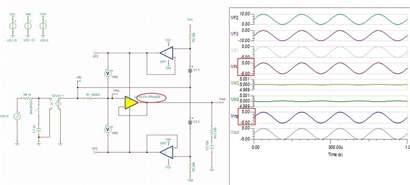
    With Cin removed, there is no attenuation of the signal in transient simulation - see below. 

    IN_BOOTSTR_OPA828 AC Response (ML).TSC

    IN_BOOTSTR_OPA828 Transient Response (ML).TSC

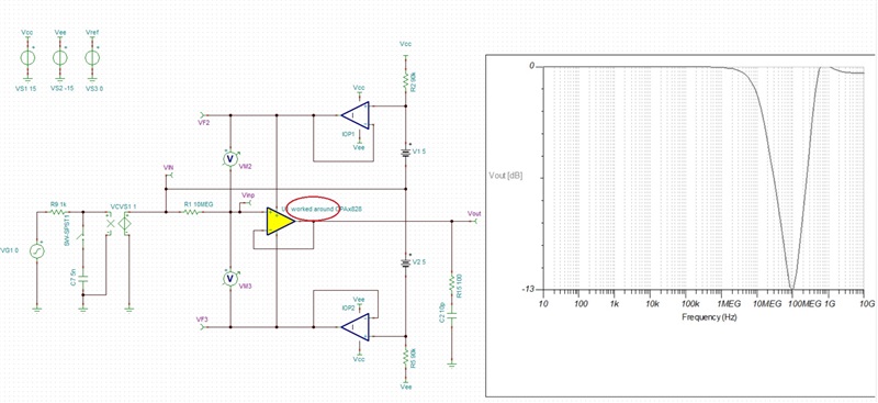
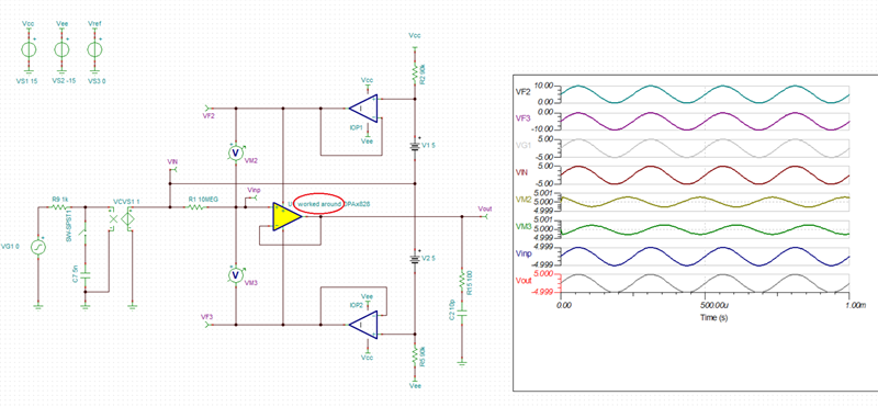
    Below I have found a work around the problem with input capacitance included.  It will be better for you to use this model for you simulations.

    IN_BOOTSTR_OPA828 work around AC Response (ML).TSC

    IN_BOOTSTR_OPA828 work around Transient Response (ML).TSC

  • Hi Marek,

    Great great thanks for both models, particularly for the work around one! Our preliminary tests show that the model with workaround behaves as expected, and both models will be very useful.

    On a related topic, we have also considered OPA192 and OPA197. The model of OPA192 exhibited similar behavior in our bootstrap circuit to OPA828 and we were unable to simulate it correctly.

    Would it be a big problem to have a similar modified model also for OPA192 or OPA197? Should we post a new thread?

    Regards,

    Michal

  • Hi Michal,

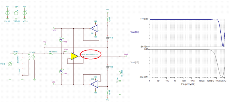
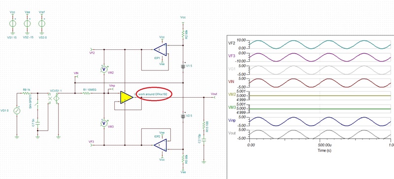
    Attached please find the OPA192 work around macro-model.  please make sure not to use it outside bootstrapping application.

    IN_BOOTSTR_OPA192 work around AC Response (ML).TSC

    IN_BOOTSTR_OPA192 work around Transient Response (ML).TSC

  • Hi Marek,

    Many thanks again!

    Regards,

    Michal

  • No problem.  Powodzenia z projektem.