This thread has been locked.

If you have a related question, please click the "Ask a related question" button in the top right corner. The newly created question will be automatically linked to this question.

PGA855EVM: Behaviour when the VICM is exceeded/ inputs saturated

Part Number: PGA855EVM
Other Parts Discussed in Thread: PGA855

Tool/software:

Hi TI,

I am trying to characterize the device behavior when the VICM range is exceeded or inputs are overloaded/saturated, specifically, what would happen to the current consumption.

The device is powered by 30V and -4V, VCC = LVDD and vice versa, gain of 8V/V. Outputs are unloaded.

I did the characterization by sweeping the differential voltage applied to inputs, with IN- at GND.

And here is the current consumption of the device.
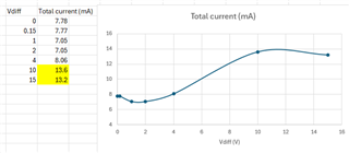
The increase in current significantly after 4V differential is concerning, because this would double the power budget, and the device would very likely interface with such voltages in end applications.

-What is happening when such voltages is applied to the device? Is the current increase expected?

-Any suggestion from TI to prevent this from happening? I think operating within the VICM is the right way, but what can I do before the input stage to operate the device better?

Thanks,

-HaoJie

  • Hello Hao,

    The quiescent current consumption specification on an operational or instrumentation amplifier represents the bias current consumption of the device while being powered at rest, without any load or input signal. However, when designing a circuit module, the designer has to create a power budget to account for the worst case loading of the amplifier, that is, the maximum amplitude and frequency signal on the system with the worst case load. 

    The PGA855 instrumentation amplifier current consumption is expected to increase with larger differential signals. This is also true for most instrumentation amplifiers, programmable gain amplifiers, or discrete gain amplifier solutions.  

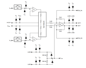
    Since the PGA855 is an instrumentation amplifier, it relies on an internal precision resistor network to produce the required gain or attenuation in the circuit. The differential input voltage is fed into a pair of matched, high-impedance input-current-feedback amplifiers. The precision-matched gain resistor network is used to amplify the differential input voltage. As the differential input signal increases in amplitude, the first stage front end amplifier feeds the differential signal into this internal resistor network. The gained or attenuated signal, then drives the fully-differential output stage amplifier, which is implemented with a network of 5kΩ resistors. The effective impedance of the gain resistor network on the input stage is in the range of a few kΩs. The input stage is designed to achieve relative low noise density at 7.8nV/√Hz; therefore, the impedance of the resistors is kept relatively low, in the range of a few kΩs to reduce the thermal noise contribution of the resistors. See figure below.

    To answer your question, most of the current consumption increase is due to the differential voltage feeding the internal resistor network and it is expected. For example, when using the PGA855 with a Gain=1, while using the device inside the valid linear operation range, applying a large differential input signal of 10V, the total overall current consumption of the device can reach around ~13mA. The current consumption increase is in part due to the current consumption on the feedback resistor network. Saturating the amplifier may also increase the current slightly. 

    The suggestion is to budget the power consumption for the worst case differential voltage on a given gain condition; and use software to detect when the output of the amplifier has reached full-scale or is overdriven, and switch to a lower gain setting to avoid saturation.  Nevertheless, the amplifier is expected to consume more current when large differential input signals are present.  Keep in mind, a similar current consumption pattern will be present on other instrumentation amplifiers, and programmable gain amplifiers that offer low noise performance, as there is a trade-off between power consumption vs noise/bandwidth performance.   

    Thank you and Kind Regards,

    Luis 


  • Hi Luis,

    Does TI have a tool to provide an estimated current draw for various signal level vs Gain settings?

    Or how should I estimate the power budget?

  • Hi Hao, 

    Most of the internal current consumption on the PGA855 with the differential signals will be through the internal resistor network at the input stage, and at the resistor network at the output stage. If the PGA855 is driving any load, the output current will need to be accounted for.  I believe the internal resistor network at the input stage has a nominal impedance around 2kΩ, and the resistors at the FDA output stage are 5kΩ each.  These resistances are accurately ratiometrically matched to provide low gain error and drift, but the absolute value of the resistances can vary a conservative ±15% over device, process and temp variation.

    We can help you with the current consumption detail.  Please confirm the details of the circuit:

    1) The supplies are +30V, -4V for both input and output stage supplies? Are there any other conditions we should estimate for?  Is the VOCM pin always biased at the mid supply or what is the VOCM voltage for each case? 

    2) What is the maximum differential input voltage and gain combinations you are using in this system?  What is the max frequency of the signal? 

    If you have an schematic showing the load, RC filters or circuit connected at the output of the PGA855, this can be helpful.

    Thank you and Kind Regards,

    Luis 

  • 1) Yes, supplies are 30V, -4V for both the input and output stgaes. VOCM pin are left floated so it should be biased at mid supply internally.

    2) Max differential voltage would be 25V, gain of 0.25V/V. We would be interested to know the condition of 25V at gain of 1 and 0.5. (We are currently stucked at this current consumption and would like to know if other gain settings have better current consumption at 25V). Max frequency is 100kHz, but how different is the current?

    3)The PGA855 would drive some other amplifier's inputs, so it's a high impedance load. No RC filters are connected.

  • HI Hao, 

    To understand the current consumption of the PGA855 device, it is easier to analyze the input and output stage of the device separately.

    - The input stage current consumption primarily changes proportional with differential input voltage for a given input common mode. There are different amplifier stages and the internal resistor network load changes slightly when using G=1 or attenuation. There is a level of dependency in the current consumption as a function of common-mode, but the current consumption is primarily a function of the differential input signal.

    - When the device is operated outside of the valid range, as long as the absolute voltage of the inputs is not overdriven and stays within the input stage supply range; there is no significant current increase.

    - The output stage is a traditional fully-differential amplifier (FDA) with a Gain of 1-V/V, therefore, the output stage current consumption can be model as a conventional FDA. The output stage gain resistor network consist of 5kΩ resistors. The output stage current consumption changes with differential signal and input common-mode fed into the second stage, as the output stage feeds the 5kΩ resistor network. 

    - The overall maximum current consumption will occur with a differential voltage of 25V while using G=1V/V.  This is because, when using attenuation of G=0.5V/V, and G=0.25V/V, the signal seen by the output stage is a smaller 12.5V and 6.25V differential voltage.  

    - If the PGA855 is only feeding a high-impedance amplifier stage, there will be little dependency on signal frequency, assuming that there is a very small or no significant capacitive load at the output of the FDA.

    I will work with design to provide an estimate for maximum current consumption. The most current consumption will be at G=1 with the 25V differential input signal; and the G=0.5V/V and G=0.25V/V attenuations will consume less power. A typical current consumption measurement with a differential voltage of 25V will be around 23.6mA at G=1V/V, 20.9mA for G=0.5V/V and 19.8mA for G=0.25V/V based on a quick bench measurement.

    Please allow a couple of business days.

    Thank you and Kind Regards,

    Luis 

  • Hi Hao,

    Discussed with the design team, were a Monte-Carlo simulation analysis and calculation was performed assuming temperature range 0°C to 80°C.

    The estimated maximum current, with VIN_DIFF=25V at 80°C, (worst case) is 27.80mA with G=1V/V

    See table below with typical and maximum estimates for G=1V/V, 0.5V/V and 0.25V/V. 

    Thank you and Best Regards,

    Luis

  • Hi Luis, thanks for the data.

    Can you also provide the estimation up to 125degC?

  • Hi Hao,

    Certainly, please find attached the table with the updated values up to 125°C.

    Please let me know if you need anything.  

    Thank you and Kind Regards,

    Luis