- Ask a related questionWhat is a related question?A related question is a question created from another question. When the related question is created, it will be automatically linked to the original question.
This thread has been locked.
If you have a related question, please click the "Ask a related question" button in the top right corner. The newly created question will be automatically linked to this question.
Tool/software:
I connected F28379D and 3PHGANINV.
F28379D to 3PHGANINV
J5 ---- J1
J7 ---- J3
J6 ---- J2
J8 ---- J4
The signal output of EPWM 1a to EPWM 3b of F28379D is designated as numbers 80 to 75 of F28379D.
The output waveform has been confirmed.
Numbers 80 to 75 of F28379D are connected to numbers 40 to 35 of 3PHGANINV.
I created a PWM signal using the DEADBAND example on F28379D. Then, I checked the output waveforms at Va, Vb, and Vc of 3PHGANINV on an oscilloscope.
There was no waveform on the oscilloscope.
Do I need to write a separate code to check the output waveforms in Va, Vb, and Vc of 3PHGANINV?
(A power supply was used as an external power source.)
I am studying the servo-Axial-drive example. Do I have to modify this example to see the output waveforms in Va, Vb, and Vc?
Hi,
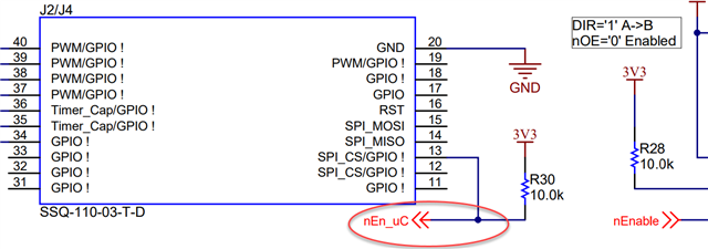
The PWM signals are buffered. Pin 13 of J2/J4 needs to provide a ‘0’ in order to enable the buffer. Here is the related schematic:

Regards,
Guang
Hi,
The uC needs to pull the GPIO assigned to pin 13 to "low". Otherwise, it is pulled up to 3.3V by default as shown in the schematic, which disables the buffer.
Regards,
Guang
I added the code below and checked the output waveform with an oscilloscope.
<<
GPIO_SetupPinMux(26, GPIO_MUX_CPU1, 0); // 3PHGANINV_ P13
GPIO_SetupPinOptions(26, GPIO_OUTPUT, GPIO_PUSHPULL); //3PHGANINV_ P13
GpioDataRegs.GPACLEAR.bit.GPIO26 = 1; // Set GPIO26 to Low
>>
Is it the right approach to write it like this??
Hi,
The best is to confirm that after the commands are executed, pin 13 is indeed pulled low. Then the PWM signals should appear after the buffer.
Regards,
Guang