AMC1311-Q1: AMC1311 distorted frequency response

Part Number: AMC1311-Q1
Other Parts Discussed in Thread: AMC1311, AMC3311, AMC1411

Tool/software:

Here is my circuit in Pspice drawing and lab experimental oscillograms,

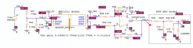
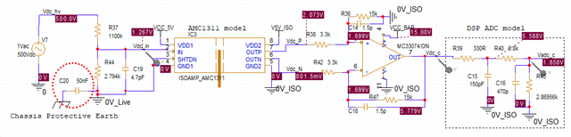
Fig 1 Pspice drawing

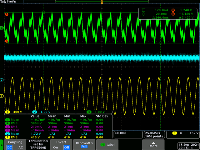
Traces in oscillograms are, 1 yellow, ac input, 2 is Vdc_hv, 3 is current, 4 is Vdc_c, only traces 2 and 4 in concern in this note. 


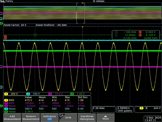
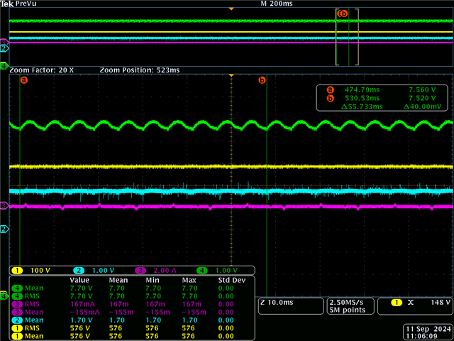
Fig 2 waveform at idle state

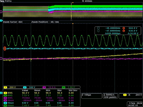
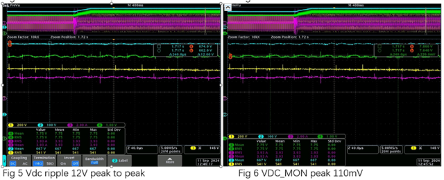
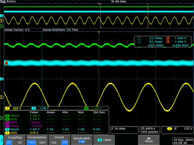
Fig 3 measured Vdc_hv ripple at 14V peak to peak

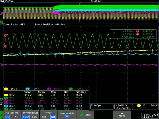
Fig 4 measured Vdc_c ripple at 1.8V peak to peak

This circuit is for Active Front End (PWM rectifier DC High voltage sensor), but it is not behaviors like simulation, it amplifies the ac components in much large gain than the dc component.

In Fig 2 idle state, the input output is stable and clean, the dc gain 6.94/589 = 0.011783. Fig 3 shows no load boost waveforms Vdc_hv ripple pk-pk 14V, Fig 4 Vdc_c ripple is 1.8V pk-pk, based gain = 7.5V/636 = 0.011792, the ripple magnitude is equivalent to 76V, not 7V in real vdc, this means that the ripple has been amplified 10 times!!!??? The true ripple should be 0.011792*7V = 0.0825V, peak to peak 0.1651V. There seems near 180 degrees phase shift.

The simulated frequency response about 200kHz width, the gain for ripple (20kHz) should be the same as dc component, but test experimental shows the ripple gain is 10 time higher.

What cause this problem, I think AMC1311 with capacitive isolation technology may too sensitive or love ac component, also I use AMC1311 for ac voltage sensor, it also has problem when power MOSFET start switching, I will talk it in another article in future. Question is, what can I do to suppress or make the ripple output on Vdc_c correct? Is this a known problem for TI?

Thank you in advance, Jian Li

  • Hi Jian, 

    Thank you for your question. We will respond shortly with recommended debug steps. 

  • Hi Alexander, many thanks for help and I am looking forward to receiving the recommended debug steps.

    Jian

  • Hi Alexander, 

      I find the cause the distorted frequency response is a 50nF Y2 capacitor C20 connected from the negative rail to protective earth (chassis) as shown below

    Remove C20 the input and output are correct as designed in AFE operation as following, (traces in oscillograms are, 1 yellow, ac input, 2 is Vdc_hv, 3 is current, 4 is Vdc_c, only traces 2 and 4 in concern in this note.) 

     However, C20 is for EMC compliance, it cannot be removed, my questions are:

     1. Why AMC1311 is affected by live side Y capacitor connection to protective earth? It is designed for isolation between the live and safe side, why it behaviors so sensitive to live side earth connection?

    2. I try to measure the input of AMC1311 with an isolated differential voltage probe, then Vdc_c oscillates as show below, (traces in oscillograms are, 1 yellow, Vdc_hv, 2 is Vdc_in, 3 is current, 4 is Vdc_c, only traces 1, 2 and 4 in concern), there is no any ripple in Vdc_hv, Vdc_in is also no ripple, why Vdc_c oscillates? AFE is not switching yet in this case. Why is it so sensitive to a measurement instrument probe? There is no connection from safe side 0V_ISO to protective earth.

    3. If C20 cannot be removed, what can I do to make AMC1311 works correctly as designed?  

    4. If AMC1311 sensitivity cannot be improved, is there any similar isolation device better immunity for my application that you could recommended?

       Thank you in advance! I am looking forward to hearing from you soon.

       Jian Li

  • Hi Jian,

    I'm glad you have been able to source where some of this error is coming from.

    To answer your questions:

    1) Comparing the first and second diagrams, are you using separate grounds for the low side and high side of the device? In the first photo, I cannot tell if it is the same ground, as this could compromise the isolation barrier. The second diagram appears to use separate grounds which looks better. High impedance devices can be sensitive to grounding. 

    2) Where are you measuring channel 4 from? Are you measuring from before or after filtering? Can you measure this channel using a ground spring (pig tail) on your probe? It might be good to ensure the oscilloscope probe ground lead is not causing measurement error.

    3) Relating to question 1 again, please make sure you are using separate grounds from high side to low side. Please let me know if this doesn't help. 

    4) If conditions do not improve after debugging, you can look through our isolated amplifier portfolio and I would be happy to find a replacement based off spec requirements: Isolated amplifiers product selection | TI.com. The AMC1411 or AMC3311 could be other options as well. 

    Please let me know if there are any other questions too. 

    Best regards,

    Eva

  • Hi, Eva,

      Many thanks for your help.

    1. This is one of my three isolated voltage sensors that employed AMC1311, 0V_live is high voltage side, 0V_ISO is Safe Low Voltage side, I am sorry that I did not mark them well in the first drawing, actually they are the same circuit, only difference is C20 that is not shown in the first drawing because I did not consider it is part of sensor circuit.

     2. The trace 4 is vdc_c measured from output of MC33074 pin 7 to 0V_ISO, that is what DSP controller received feedback. 0V_ISO is not grounded to chassis, measured signal from vdc_c to ground is not true signal that DSP controller sees, AMC1311 output is differential, it should not be affected by grounding as this isolated IC is immune or very little affected by common ground interference, am I right? 

    3. Yes, they are two separated grounds, about 700Vdc difference.

    4. AMC1411 is the same footprint, I will try to study and buy and replace AMC1311. 

     Thank you for various suggestions!

      Jian Li

  • Hi Jian,

    Thank you for your reply and for clarifying these points about your circuit. So, trace 4 is the differential to single-ended conversion output at pin 7 of the MC33074. I think you should still measure this output with reference to ground to evaluate. More debugging advice would be to also measure the differential output of the AMC1311 before the op amp. This would help determine if the ripple is first seen after the device or after the op amp.

    If you do decide to try an alternative device, please let me know if there are any more questions for getting started there too. 

    Best regards,

    Eva

  • Hi, Eva, 

     Here are two oscillograms when a differential probe is put on AMC1311 input, (traces defintions, 1 is Vac, 2 is Vdc_in  on pin 2 of AMC1311, 4 is vdc_c on MC33074 pin 7. The first one below is measured from Vdc_c respect to 0V_ISO, as the same as before on Sept 11, the second one is measured from vdc_c to ground (chassis).  Clearly it is worse.    


        AMC1411 has different package, and longer body does not fit in AMC1311 footprint. I think AMC1311B may worth a try as it is better than AMC1311 and exact the same footprint. There are a few MC33074 on my board as part of current and temperature sensors, without such oscillation problems. I do not think it is part of problem in this Vdc sensor. 

  • Hi Jian,

    Okay, the AMC1311B does typically have better performance than the AMC1311, so this would be a good alternative device. Please let me know if you have questions about the AMC1311B or getting started.

    Best regards,

    Eva