This thread has been locked.

If you have a related question, please click the "Ask a related question" button in the top right corner. The newly created question will be automatically linked to this question.

LMH7322: Implementation fault

Part Number: LMH7322

Tool/software:

Hi, and thanks for reading this!

I have a PCB where a custom chip produces four LVCMOS 1.2V outputs - named OUT_0, OUT_1, OUT_2, OUT_3 - which I had to convert to LVDS. I considered implementing two LMH7322SQ/NOPB comparators with 0.6V reference voltage to do this. However, the outputs are stuck just above 1V. My implementation is the following (identical for the two comparators):
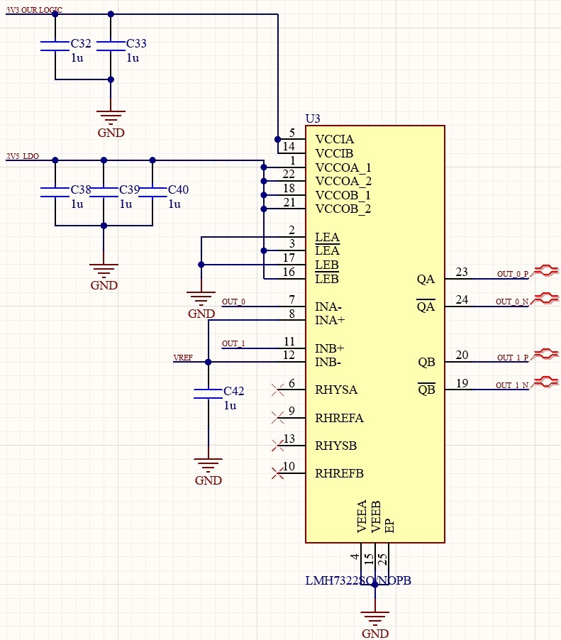
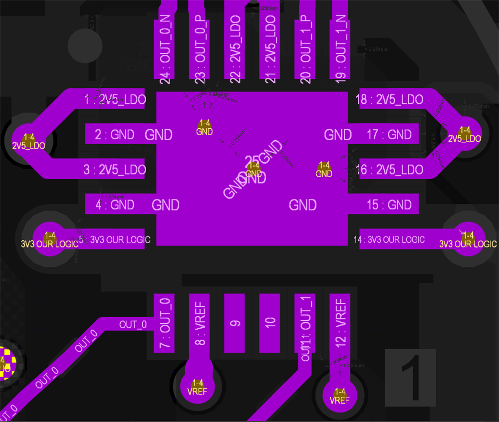
All voltages are set correctly.

I know pins 6 and 13 are missing. That was my doing, as I did not want any hysteresis I left them unconnected (and tried to get a signal going under the chip, but didn't do it in the end). I suppose the problem is not connecting any resistance to pins 2 and 3 (I did not want any latching function)., but I'm not sure.

Thank you for your time!

MR

  • Hi Marco,

    What values for termination resistors are you using for the Q and Qbar outputs? In addition, how are these termination resistors connected and how are you measuring the outputs (oscilloscope or DMM?)

  • Hi Ho! Thanks for helping!

    To clarify, the system is composed of three stacked boards: carrier, power and FPGA (from top to bottom). The comparators are soldered on the top of the carrier, and their output reaches the FPGA. Q and Qbar are connected via a differentially controlled impedance (100 Ω) trace to the carrier's board connector (ERM8-030-05.0-L-DV-L-TR, found on the carrier's bottom layer). This is connected to its female on the power board (ERF8-030-05.0-L-DV-L-TR, found on the power's top layer), which delivers the signals again through differential traces with impedance control to a third connector (BTE-040-01-F-D-A, found on the power's bottom layer). This third connector delivers the signal to an Opal Kelly XEM7310-A75 which can be differentially terminated but has not been in the tests we have done.

    The pins used in the FPGA are:

    • MC2-37 and MC2-39
    • MC2-23 and MC2-25
    • MC2-46 and MC2-48
    • MC2-38 and MC2-40

    refer to (https://pins.opalkelly.com/pin_list/XEM7310) for further information.

    To probe the outputs we are using an oscilloscope, inserting grounding one probe and placing the second in the carrier's vias (needed to get the Q and Qbar from the top to the bottom connector).

    Feel free to ask any other questions!

    Thank you!

    Marco

  • Hi Marco,

    Thanks for the detailed explanation. From what I understand, the outputs Q and Qbar are both connected through traces and board-to-board connectors into the pins of the FPGA. From the schematic alone, the latch logic should be fine, and the comparator should be configured to work continuously. Connecting resistances to the latch pins are meant to protect the pins from overcurrent.

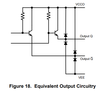
    The LMH7322 outputs are open emitter:
     

    LMH7322 does not have true LVDS outputs. It's using the VCCO = 2.5V on an RSPECL output to mimic LVDS logic levels: (VOH = 1.4V, VOL = 1V from VCCO - 1.1V and VCCO - 1.5V). Both outputs need termination resistors to VEE in order for the outputs to swing.