- Ask a related questionWhat is a related question?A related question is a question created from another question. When the related question is created, it will be automatically linked to the original question.
Tool/software:
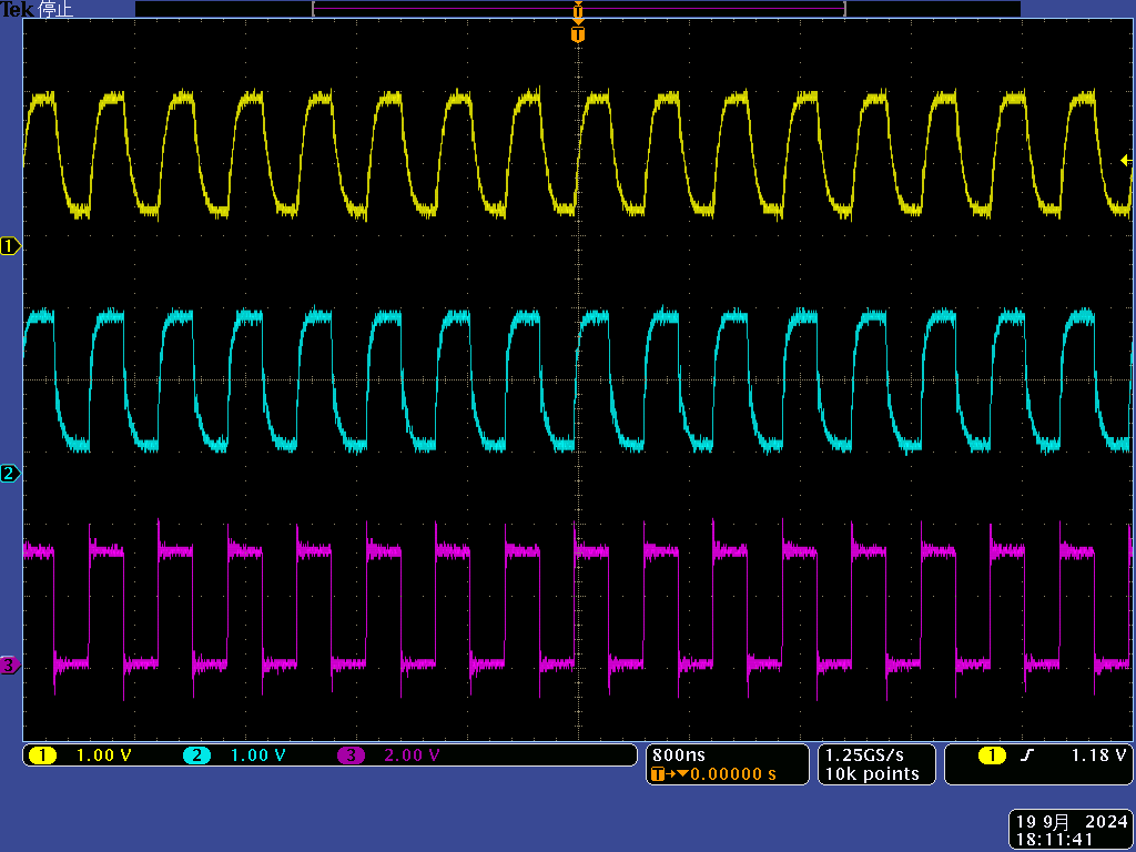
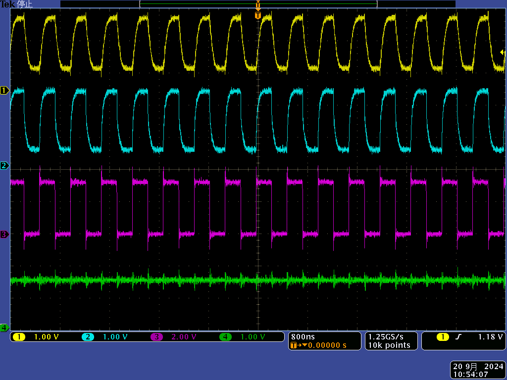
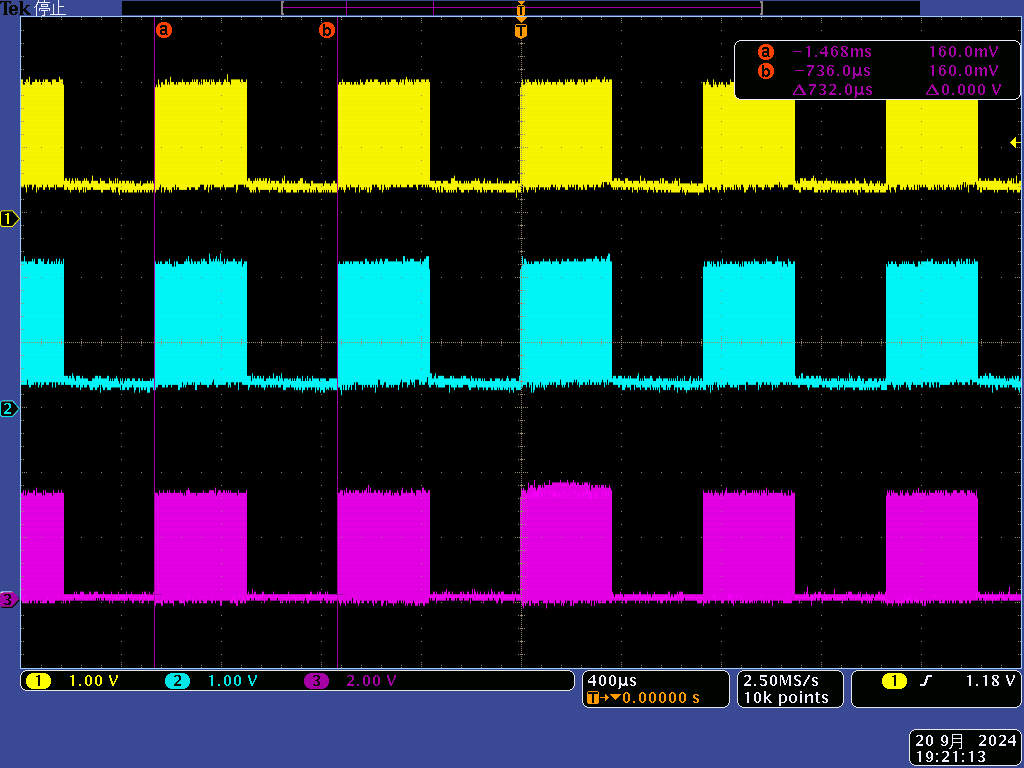
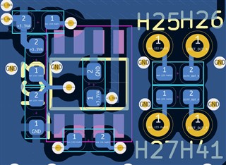
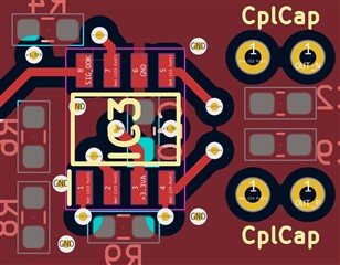
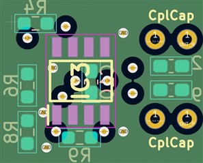
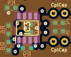
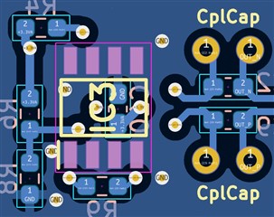
It is not a differential output.
Signals in-phase are output.
What is the cause?
CH1:DIFF_OUT_N
CH2:DIFF_OUT_P
CH3:DIFF_IN