Because of the holidays, TI E2E™ design support forum responses will be delayed from Dec. 25 through Jan. 2. Thank you for your patience.

This thread has been locked.

If you have a related question, please click the "Ask a related question" button in the top right corner. The newly created question will be automatically linked to this question.

LMP2012: Thermocouple amplifier produces DC offset with 100kHz interference

Part Number: LMP2012
Other Parts Discussed in Thread: REF3040

Tool/software:

Shown below is a thermocouple amplifier circuit implemented using the LMP2012.
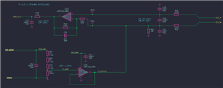
Using K type thermocouple, the circuit produces the expected response of ~2.77mV/°C. (gain of 67.67)

In the same system there are PWM controlled valves. When the valves are actuated, and the wires of the valves are routed close to the TC wires a DC offset is produced on the output of the amplifier. This varies between units but can be up to 120mV (~50C measurement error).

Removing C12 appears to dramatically reduce the effect but not totally eliminate it.

My question is what is likely cause of this susceptibility?
What can be done to mitigate this effect further?

  • Hi Marcus, 

    Using K type thermocouple, the circuit produces the expected response of ~2.77mV/°C. (gain of 67.67)

    For K type TC, 0C is 0mV and 100C is 4.096mV or the slope is 0.04096mV/C from 0-100C. The slope is positive. 

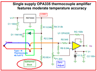
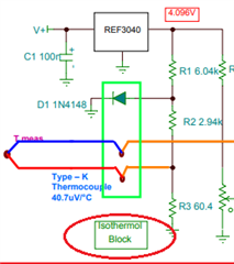
    The isothermol block or cold junction block has to come from bandgap reference voltage, such as REF3040. The isothermol block has to be stable over temperature, otherwise, you will not be able to measure the TC's voltage difference vs. temperature. 

    Please pay attention to the color code of the following diagram, red, blue and orange leads, because red and orange leads have polarity differences, and should not connect it backwards. 

    The TC's circuit with cold junction or electronic voltage reference should look like the following, see the application reference below. 

    https://www.ti.com/lit/ml/slyp161/slyp161.pdf

    https://www.ti.com/lit/an/sbaa274a/sbaa274a.pdf?ts=1727821705194&ref_url=https%253A%252F%252Fwww.google.com%252F

    https://www.ti.com/lit/an/sbaa354a/sbaa354a.pdf?ts=1727819827119

    Please simulate the above circuit and see if it works for you. What is your K type TC's design accuracy? What is temperature operating range?

    If you need additional questions, please let us know. 

    Best,

    Raymond

  • Hi Raymond, 
    Thank you for the reply.

    In this application we are using a thermistor for cold junction compensation which is not in the scope of this discussion.
    The amplifier works as intended, note my use of "~" here is not a minus sign. The amplifier output is approximately 2.77mV/°C which is simply the TC slope times the gain (0.04096mV/°C * 67.67 = 2.771763mV/°C) 

    The issue I am trying to solve is that the circuit is susceptible to 100kHz interference. We experience the measured temperature increasing when the interference source is enabled.
    I have since isolated the problem to the unity gain op-amp which produces a 0.375V offset on the negative lead of the TC (TC_OFFSET in the schematic).
    The average voltage on the output of the unity gain amp appears to increase when a 100kHz signal is capacitively coupled to the TC_N or TC_P net.
    The average voltage on the input to the unity gain op-amp (TC_VREF in the schematic) does not change.


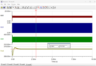
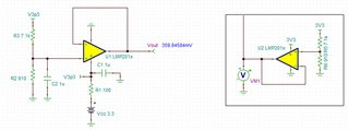
    Simulating the circuit in TINA with noise coupled onto the does not show this effect. The average voltage on the output is 0.37418V in TINA, yes the TC_OFFSET as simulated is quite noisy but the RC filter on the output does a good enough job of smoothing that out as expected.


    What may be causing the unity gain amp to produce a higher average voltage on the output when there is an AC coupled interference?

    How does reality differ from the simulation in this case?

    Thanks,
    Marcus

  • Hi Marcus, 

    The issue I am trying to solve is that the circuit is susceptible to 100kHz interference. We experience the measured temperature increasing when the interference source is enabled

    Are you using switching power supply for your TC sensing circuit? I assumed that 100kHz is from the switching power supply. 

    How is the 3.3Vdc obtained? If it is from a switching power supply --> LDO --> 3.3Vdc low ripple voltage DC source. Please confirm. 

    Is the GND is isolated from 100kHz switching power supply?

    I need to know these parameters in order to troubleshoot the noise issues. What is the ripple voltage at 3.3Vdc? It should be less than +/-10mVpp or better at high frequency.

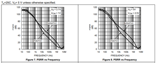
    Where did the interference source is applied? The noise source could go through the 3.3Vdc and showed up at the amplifier's output. There is approx. 20dB attenuation in PSRR at 100kHz from the plot below. 

    Simulating the circuit in TINA with noise coupled onto the does not show this effect. The average voltage on the output is 0.37418V in TINA, yes the TC_OFFSET as simulated is quite noisy but the RC filter on the output does a good enough job of smoothing that out as expected.

    The noise interference may not come from the TC, since it is low impedance and you have differential and common mode LPFs at the input. I do not believe that the 100kHz noise is entered from the TC front end. 

    What may be causing the unity gain amp to produce a higher average voltage on the output when there is an AC coupled interference?

    Try the following configuration, if your 3.3Vdc rail is noisy with high ripple voltage. Use low ESR capacitor to see if the system has noisy 3.3Vdc rail. 

    I need to have more information about an AC coupled interference? How is done and where the noise source is from? I am just guessing currently. If your 100kHz noise is a radiated source, please check the 3.3Vdc supply when it is turned on. Check for the ripple voltage with scope at the op amp's supply rail (next to the pin and bypass capacitor). 

    I assumed that your TC measurement is working, except the high frequency noise issues. The TC connection has to be terminated in isothermal block, shown in green box (cold junction temperature block) below. The isothermol block is the temperature reference and the voltage reference can be measured via thermistor, RTD, PN Temp sensor or simply ice bath (the voltage equivalent to the temperature of the cold junction). I just want to make sure that you do not have configuration issues with the measurement. The noisy issues are stated above, but I need more information about how your 100kHz interference is conducted.  

    If you have other questions, please let me know. 

    Best,

    Raymond

  • Hi Ramond, my apologies for the delayed response.

    The PCB which implements the TC amplifier also supplies 32V to a load which is low side switched at 100kHz.
    This is shown in my TINA model as the 33mH + 34ohm with capacitive coupling to the TC lines.

    The system is supplied with 32V and 5V by two separate supplies both referenced to ground. The 5V input is regulated to 3V3 with an LDO and the 3V3 rail supplies the amps continuously. The 3V3 is also the ADC reference voltage on a MCU and is responsible for sampling many other signals on this design which work well even when the PWMs are running which leads me to believe that the 3V3 supply is not the issue. 

    After a lot of messing around with this issue I have established that placing the PWMed conductors perfectly in parallel up against the TC wires produces the offset. A ground connected metal foil between the two completely eliminates the issue. Increasing the distance between the parallel conductors is also effective to eliminate the offset.

    The offset as a function of length of parallel conductor is linear with length of parallel conductor until at a critical length the interference suddenly jumps to much higher level and will not return to the previous levels till the length is decreased significantly further. There appears to be a secondary

    Below images show the shield connected and not connected (its a little hard to see in the second image that the shield is disconnected but trust me it was). Sorry for the poor quality, these images are taken from a video. In this scenario the critical length is exceeded, and the oscillations are large.  The scope ground used is approximal 5mm long. A twisted piece of wire is used instead of a TC so there are no temperature effects.
    The amplifier output is in green and shows a DC increase between the two images. The noise source is used to trigger the scope (blue trace) the TC offset net is probed for the yellow trace. Oscillations are 300Khz (3x PWM freq). 


    My question are, why does this (relatively) high frequency interferance on the input produce a DC offset on the output of the amp? the RC filter on the output has a cutoff of ~1kHz.
    Why does this not match the simulated results?

  • Hi Marcus,

    If you are using LDO to generate 3.3Vdc for the op amp, the op amp's supply rail is likely ok. 

    How do you dealing with GND? To need to terminate all ground connection to a single point, and that ground point needs to be tied to Earth GND, including your 100kHz radiated source.

    Since you using 100kHz switching power supply, I would isolate the op amp's analog GND from Switching Power supply's GND. Use thinner or higher gauge wire, say #28 or #30 gauge wire to connect to the single GND point (the increased analog GND impedance should be higher than the switching power supply's GND (thicker GND and lower gauge wire). 

    In the simulation, the common mode noise is identical and that is why you are unable to simulate it. In actual setup, it is likely that the common mode is converted in the differential input signal, and you start to observe the offset voltage when you radiate your 100kHz signal in certain ways. 

    I noticed several things in the attached image. 

    a. There should be isothermal block where different TC metal is terminated to copper wire. You need to make sure that isothermal block is stable and outer block is terminated to GND. Ideally, this isothermal block should be closely tied to the measurement circuit or the op amp circuit. The white wire is likely your Cu leads, it is hard to say where the TC and TC metals/Cu termination is. In the previous reply, the terminated block is shown in green box. 

    b. Use twisted pair TC and Cu wire leads.  Your Cu leads are not twisted pair type. 

    c. Use GND shielded TC and coaxial Cu cable, which will reject the radiated noise better than bare wire. 

    d. Your LPFs should be placed close to Op amp input circuit. I do not know where it is. 

    e. Configure your TC as Faraday cage, which it can block the radiated emission from your noise sources. 

    The noise source is used to trigger the scope (blue trace) the TC offset net is probed for the yellow trace. Oscillations are 300Khz (3x PWM freq). 

    The op amp has certain PSRR rejection against 100kHz noise, but it has no rejection against the odd harmonics noises, say 300kHz. It is possible that it goes through the power pin from there or coupled in via the Vref signal of the difference amplifier. 

    Anyway, I listed several areas where the radiated noise may be coupled into the system. You may need to use low ESR capacitor to decouple these noise sensitive nodes and make your system better in rejecting the radiated noise. 

    Is your 100kHz noise source generated from 100kHz square wave?

    Please let me know if you improve the noise rejection from the suggestion. If you are unable to reject the noise effectively, you may have to use instrumentation amplifier for the TC's amplification front stage.

    If you have other questions, please let me know. 

    Best,

    Raymond 


  • Hi Marcus,

    I am going to close this query. I assumed that your issues are resolved.

    If you have additional questions, please let me know. 

    Best,

    Raymond

  • Sorry for the lack of interaction. There have been other priority issues for me.
    I did end up resolving the issue in two ways.


    1 - Implementing shieling between the noise source and TC conductors.

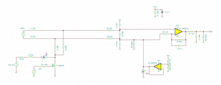
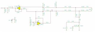
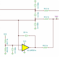
    2 - Modifying the circuit to be less susceptible, see below. 

    Both are effective in practice; however, the modification of the circuit also resolved a secondary issue where this circuit was also susceptible to 50Hz main interference when the TC was attached to larger floating or poorly earthed metal objects.

    I am still interested as to why the output of my simulation of the original circuit did not match reality, why do we see a DC offset on the output of the amplifier when there is ripple on the input? The AC transfer characteristics show these frequencies should be attenuated greatly.

  • Hi Marcus,

    why do we see a DC offset on the output of the amplifier when there is ripple on the input?

    I do not know what your TC accuracy specification is. The ripple noises at the input is likely from the following components. 

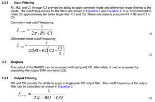
    a. 50Hz coupling noise: the differential LPF filter needs to be lower, from 5Hz to 10Hz range. You had better differential and common mode filter configurations, see the image below. The common mode LPFs should be placed at least a decade after the differential LPF. 

    https://www.ti.com/lit/ug/sbou115c/sbou115c.pdf?ts=1729085312089&ref_url=https%253A%252F%252Fsearch.yahoo.com%252F

    b. Please make sure that the supply rail 3.3V has low ripple voltage, <10mVpp or better (depending on  your system's accuracy requirements). 

    c. The Isothermal block needs to be temperature stable, within ±0.1C or better over temperature. Otherwise, you may observe Seebeck's effects. 

    d. U2 may need to use Bandgap reference instead of voltage divider reference. REF3040, REF35 or similar voltage references may work better. 

    https://www.ti.com/power-management/voltage-reference/products.html?keyMatch=voltage%20reference%20selection&tisearch=universal_search

    I am still interested as to why the output of my simulation of the original circuit did not match reality,

    You may need unbalance the parasitic L and Rwire effects at the input, convert the common mode noise to differential signal. Your filtering is already low around 8kHz, so anything you injected has to be below or near the cutoff frequency. Otherwise, the injected high frequency will be greatly attenuated. 

    Please let me know if these suggestion helps. If you have other questions, please let me know. 

    Best,

    Raymond