This thread has been locked.

If you have a related question, please click the "Ask a related question" button in the top right corner. The newly created question will be automatically linked to this question.

OPA316-Q1: Please tell me what needs to be done for getting the expected output

Part Number: OPA316-Q1
Other Parts Discussed in Thread: INA180-Q1

Tool/software:

Hello,

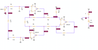
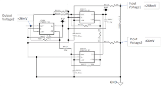
My customer is investigating OPA316-Q1 and they expect the output shown below from the attached schematic, but they got much lower voltage.  Would you please tell me what they need to do?  Note that the common mode voltage is -0.2V~+0.2V, so the input voltage should be OK.

Expecting output = 10 x (InpVol1 - InpVol2) x (1+2 x (10k/10k)) x (75k/10k)

* In case if the schematic isn't clear enough, R is either of 0.2/4.3k/10k/75k and C is either of 0.01u/0.1u.

Best Regards,

Yoshikazu Kawasaki

  • Hello Kawasaki-san,

    What is connected on the output of the final amplifier?

    Also please confirm my below circuit matches the above configuration. I have not place capacitors on the supply pins as this is an ideal simulation, so they are not needed.

    Best,
    Jerry

  • Hello Jerry-san,

    Thank you very much for your quick reply.

    I'm not sure what is connected to the output, but your ideal simulation doesn't show the low voltage like my customer found.  They checked the output voltage on their board using the actual OPA316-Q1 devices.  Their circuit shouldn't violate the datasheet.  Would you please tell me what the root cause would be?  What do you think they should do to have the expected output?  Do they need amplifiers supporting +/- voltage instead of single supply of 5V like this time or current sense amplifiers like INA180-Q1?

    Best Regards,

    Yoshikazu Kawasaki

  • Hello Kawasaki-san

    I am asking what is connected to the output of the final device to try to determine the root cause, as it is not immediately apparent from just the information you have shared.

    Does the customer have the voltage reading from the output of each op amp?

    Additionally, if ground is 64mV, the output of the final amplifier should not be able to be below V-. This is why I am asking what is connected to the load, as the op amp should not be able to drive below V-.

    Best,
    Jerry

  • Hello Jerry-san,

    Thank you for your reply.  The load should be ADC to monitor the voltage from the output of this circuit.  Would you please tell me what the root cause would be?

    Best Regards,

    Yoshikazu Kawasaki

  • Kawasaki-san,

    My apologies, it appears I am not being specific enough. Can you please tell me all the components that are connected to the output of the amplifier, starting from the amplifier output pin and ending with the ADC input pin. Please list all resistors, capacitors, and other components. A schematic would be most helpful in identifying this.

    Additionally, can the customer measure the voltage at the output node of each amplifier in addition to the inputs to the first stage and the final output?

    Best,
    Jerry

  • Hello Jerry-san,

    I'm sorry that I wasn't understandable enough.  ADC will be directly connected from the final amplifier output without any components like resistors or capacitors.  The outputs of the other amplifiers aren't monitored.  All the connections are shown in the gif file in my first post.  Would you please tell me what the root cause would be?

    Best Regards,

    Yoshikazu Kawasaki

  • Hello Kawasaki-san,

    As specified in my previous post, if the circuit is configured exactly as shown, it is not possible to have that output on the amplifier, and the error must be somewhere else. If the GND node has seen a shift of 64mV, and this same 64mV is seen at all 3 amplifiers, it is not possible for the final amplifier to output a voltage of 26mV. An op amp is not capable of driving an output outside of the supply rails.

    This must mean that the information provided initially is incorrect, as it is not possible to operate otherwise.

    This could mean a ground shift between the op amp ground and the ground of the shunt, or some other issue going on in the circuit.

    Best,
    Jerry

  • Hello Jerry-san,

    Thank you for you rcomments.  I know it's not possible to drive the external ADC by 26mV.  However your ideal circuit has >2.0V output.  That's why I'm asking what the root cause would be.  You mentioned it could be ground shift or something, but does OPA316-Q1 wolr even if the Vcm=0 or so by Vdd=5V?  Can OPA316-Q1 work such tough conditions?  Don't you have issues like my customer in the past?  What do you need from my customer to find the root cause?

    Best Regards,

    Yoshikazu Kawasaki

  • Kawasaki-san,

    I am saying that the data provided by the customer cannot be correct.

    If the orientation of the current is opposite from what they are expecting, the output would be close to V-. However, the information that has been provided by the customer cannot be true.

    This is because this analysis is based on two assumptions. The first is that the customer configured the circuit the same in their schematic as they did in their circuit, and the second is that their measured node voltages are correct. However, if the customer has configured the circuits exactly the same as the above circuit, the second assumption cannot be true.

    It is possible that the circuit is configured incorrectly, a device was damaged in some other use case, or that some other error was made, but it is not at all possible for V- of the amplifier to be 64mV, and the output of the amplifier to be 24mV.

    I am requesting that the customer check their configuration and remeasure the node voltages. Please request that they measure the output voltage of each amplifier, not just the final amplifier. Also please ask the customer to measure V- at each amplifier pin.

    Best,
    Jerry

  • Hello Jerry-san,

    We did some simulations and found the root cause of the issue.  The low side input amplifier expects output of <0V, so it can't do that unless they use minus power supply.  We sent the results with alternative solution with INA devices to our customer and haven't received any replies since then.  Please let me close this thread and open another one if we get additional issues or questions.

    Best Regards,

    Yoshikazu Kawasaki

  • Kawasaki-san,

    Thank you for providing the information to close this issue.

    Best,
    Jerry