This thread has been locked.

If you have a related question, please click the "Ask a related question" button in the top right corner. The newly created question will be automatically linked to this question.

TLV2372: TLV2372

Part Number: TLV2372
Other Parts Discussed in Thread: TLV9002, TINA-TI

Tool/software:

Hello TI Team ,

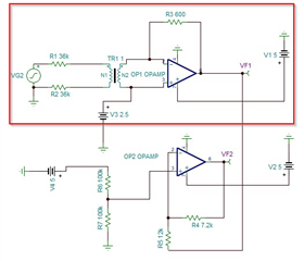
We are experiencing some confusion in properly setting the gain for our circuit. Could someone please assist us in adjusting the gain for the attached circuit? Additionally, we would appreciate it if you could verify whether the attached waveform and circuit are correct.

Furthermore, could you provide the correct procedure for simulating the circuit and obtaining the correct waveform?

Thank you for your help!

  • Hi Deepika, 

    Welcome to E2E! 

    Could you clarify what gain you are trying to set? Is it for the first stage? What is the intended output waveform you are looking for? 

    Also, I noticed you are using the ideal amplifiers in the simulator. Are you are trying to design this with the TLV2372? 

    Regards,
    Ashley

  • Hi 

    Here is the Input Information for clarification:

    • Input current max = 3mA and min = -3mA of a sine wave.
    • Vout for current max of 3mA = -I × Rf = -0.003 × 600 = 1.8V
    • Vout for current min of -3mA = -I × Rf = -0.003 × 600 = -1.8V
    • The input offset is 2.5V, so it should vary from 0.7V to 4.3V with 2.5V as the center.

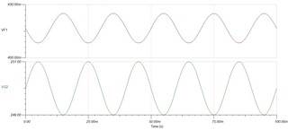
    However, the expected Vout is not appearing. Instead, we are observing the following waveform from our simulation.

    Simulated Output Explanation:

    1. VF1 (Top Waveform):

      • We are seeing a voltage fluctuation between 400mV and 430mV. This is much lower than the expected ±1.8V, indicating a gain issue or an offset voltage problem. The amplifier does not seem to be providing sufficient amplification as expected.
    2. VG2 (Bottom Waveform):

      • This waveform represents the input signal, which is oscillating between 249V and 251V. However, this discrepancy further suggests that the output is not behaving as it should.

        We summarize this information as Follows :

        • The expected output is between ±1.8V based on our calculations (with input current of ±3mA and a feedback resistor of 600 ohms).
        • However, the actual output waveform in the simulation does not match this expectation. Instead, VF1 is showing significantly lower voltage.
        • Please verify whether the circuit’s gain configuration is correct and whether the op-amp model used in the simulation could be causing these discrepancies.


        Thanks And Regards ;
        Deepika R
  • Hi Deepika, 

    Could you share your simulation file and clarify a few points below: 

    Input current max = 3mA and min = -3mA of a sine wave.

    Where is this current source coming from in the application? 

    What is the intention of the transformer? I'm not sure if the gain of the op amp is used correctly if you are trying to gain with the transformer? The circuit initially looks like a difference amplifier circuit with some resistors missing - is this the application design? 

    Regards,
    Ashley

  • Thank you for voltage sense final 1.TSCcurrent sense final 1.TSCyour observations. We have a similar circuit for current sensing with the same input current (Input current max = 3mA and min = -3mA of a sine wave). However, in that circuit as well, we are not obtaining the desired output waveform.

    To clarify further:

    1. The input current source comes from an external signal generator in the application.
    2. The transformer is intended for voltage isolation and signal conditioning, though we are reviewing its effect on the op-amp gain.
    3. The design you mentioned resembling a difference amplifier is intentional, but we are reviewing the resistor values and placement to ensure proper operation.

    We will continue to investigate the issue and adjust the circuit accordingly. Please let us know if you have any additional insights on this.

  • Hi Deepika, 

    Thank you for the TINA simulation files. Here are a few additional comments from my end: 

    • If you are trying create a current sensing circuit, we have many circuit resources in our Analog Engineer's Cookbook: https://www.ti.com/design-development/analog-circuits.html
    • If you are trying to simulate a current input, I recommend to instead use a current source in simulation. Currently what I am seeing now is only a DC input in your simulation files. 
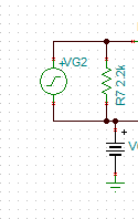
    • When you use a voltage input signal source, you cannot connect it differentially like this: 
      • There needs to be ground connected to the negative side. 
    • I recommend to download the latest TINA model from the product page of the op amps you are trying to simulate. The TINA library is not the latest versions of the models and we keep the latest versions available for download on the product page. 

    Please let me know if you have further questions.
    Thank you!

    Regards,
    Ashley

  • Dear

    Thank you for your earlier response regarding our simulation, where you suggested using a current source instead of a DC input. We implemented the correction as recommended and are now getting the desired output for IG1, which is within the expected range of +3mA to -3mA.

    However, we are encountering an issue with VF2. Theoretically, we expect to get 3.4V at VF2, (Formula : VF2= I x Rf + ref voltage) based on the following:

    - Input current: 3mA
    - Feedback resistor: 600Ω
    - Reference voltage: 2.5V

    Despite this, we are observing only around 2.9V in the output, and it appears to be clamped. Could you please guide us on how we can eliminate the clamping and achieve the correct output?

    Additionally, we would appreciate your assistance in understanding how to correctly set the gain and resistor values to get the desired output of 3.4V.

    I’ve attached the circuit and waveform for your reference.

    Looking forward to your insights.

    Regards:

    Deepika R

    Current Sense.TSC

  • Hi Deepika, 

    The clamping behavior in your current simulation is due to the op amp that was chosen. The op amp in the schematic is the LM301A, which has limited output swing range from the rails. Since you are using the part with 5V supply, this range will be smaller and be clamped at about 3V. 

    When I change it to the TLV9002 and ground the input current source, this is the transient response: 

    Which op amp are you wanting to use in your application? We can to help to recommend a suitable option depending on your application conditions and package needs. 

    Regards,
    Ashley

  • Hi ,

    Thank you for your feedback regarding the clamping behavior in our current simulation. We attempted to implement the suggested part (TLV9002) in place of the LM301A op amp; however, we are unable to locate the TLV9002 in our simulation tool's library.

    Could you kindly guide us on how we can add this part to our simulation tool? If there are specific steps to follow, we would appreciate your assistance in providing those instructions.

    Looking forward to your response.

    Thanks And Regards ;
    Deepika R

  • Hey Deepika,

    I will help support this thread while Ashley is out of office. 

    Please navigate to the product page for TLV9002 and scroll down to "Design and Development" and select "Design Tools & simulation"

    Here you will find both the TINA model and the reference design:

    The reference design will be an existing project with the model already imported. The TLV9002 TINA-TI Model will be a .TSM file, allowing you to easily add the macro model into any project you want via the TINA-TI Insert Macro option".

    Please let me know if you have any questions,

    Best,

    Jacob