This thread has been locked.

If you have a related question, please click the "Ask a related question" button in the top right corner. The newly created question will be automatically linked to this question.

LM331: Design considerations and response when used as isolation amplifier

Part Number: LM331
Other Parts Discussed in Thread: VFC110, VFC32, VFC320

Tool/software:

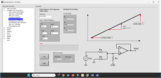
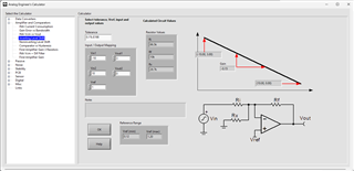
I plan to use LM331 as an isolation amplifier in a way similar to figure 4 of this application note:

https://www.ti.com/lit/an/snoa819/snoa819.pdf

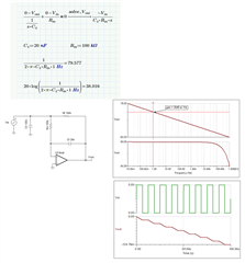
What kind of bandwidth can I get from this circuit? Considering the 100kOhm/0.1uF LPF at input, my guess would be in the range of tens of hertz. Is this correct?

Is there a way to extend the bandwidth to at least 1-kHz, preferably several kHz?

According to page 15 of the LM331 datasheet:

https://www.ti.com/lit/ds/symlink/lm331.pdf

In this kind of V to F and back to V system, the bottleneck to fast response is actually the LPF on the output side, for converting received pulses into a smooth output voltage. If this is the case, can I select a higher frequency to lessen the filtering requirement and improve response? For example, can I design the V to F stage so the full input range corresponds to ~90 to 100 kHz instead of 10 Hz to 11 kHz? By doing that, I only need a filter for 90 kHz instead of 10 Hz, which should greatly improve response.

Also, is figure 4 in the aforementioned application note (or figure 19 in the datasheet) inverting? since output of LM331 is connected to the inverting input of the op amp. If yes, is there a way to make it non-inverting? Is this op amp configured as a transimpedance amplifier, since output of LM331 is current pulses rather than voltage pulses?

Thank you

  • TI no longer makes the LS-400, but more moden phototransistors have the same physical limits and are not any faster. With a 10 kΩ load, more than 1 kHz is doubtful.

    You could try to use a photodiode and amplify its output, but then it would be easier to use an integrated isolated amplifier.

  • Phototransistor or optocoupler is not a limiting factor for me. I have other means of getting the pulses across the isolation barrier that is much, much faster than phototransistors. The inherent limitation of LM331 itself is the limiting factor for my system. So it would be extremely helpful to know how to optimize LM331 based V to F and F to V converter for faster response.

    My input and output sides would  NOT be on the same board. I do not think an integrated isolation amplifier would be useful for my case.

  • Hsin-Che,

    Typically, the maximum frequency of a VFC is not adjustable in monolithic Voltage-to-Frequency converters.  The VFC32 allows for a much wider frequency range.  Can you use this device?  I do see also VFC320 and VFC110 for voltage to frequency operation, but these devices are only available in PDIP format and the VFC32 is available in SOIC.  

    Best regards, Art

  • I am not trying to exceed the maximum frequency. Page 1 and 3 of the LM331 datasheet say that the maximum frequency is 100-kHz, but the example circuit provided (e.g. Figure 14 on page 12) is only 11 Hz to 10 kHz for the full input range. Why? Can I change it to, for example, 90kHz to 100 kHz, or 50+-5 kHz, or any other frequency range within the 100-kHz limit?

    If this is possible, then how do I modify the receiving (F back to V) side to accommodate for this change in offset? I see an offset adjustment potentiometer on the V to F circuit (Figure 14), but not on the F to V circuit (Figure 18 and 19). Is it possible to include an offset adjustment on the F to V side?

  • Hsin-Che,

    Figure 17 illustrates the circuit for a 100kHz full scale output frequency range.  Figure 7 illustrates the non-linearity error for this circuit for the 100kHz range.  The inherent operation of the circuit is to range the output frequency starting near zero and ending at the full scale frequency.  You can use a level shift amplifier to force the LM331 input signal range to meet your output frequency requirements.  For example, if your natural input range (e.g. DAC output) is -10V to +10V, you could shift this to be -10V to -8V when the input is -10V to +10V.  You could do a similar level shift on the receive side (F-to-V).  Tools to find components for inverting and non-inverting level shift are available in the analog engineers calculator (see below).  Note that this circuit will have good linearity, but the absolute accuracy is limited (gain specification "conversion accuracy" is +/-5%).  The gain error limitation is why the original document has the trip potentiometers.  If you adjust the range to 90kHz to 100kHz you will likely need to do some kind of calibration to account for this inaccuracy.  I suggest prototyping this circuit since we do not have models to test the circuit. 

  • Thank you so much for pointing out Figure 17 in the datasheet. How do I miss that! I suppose the extra components (OP amp and transistor) is for improving linearity and I can still use the basic circuit (Figure 14) to get whatever frequency range I want, just by playing with the RC values, right?  However, minimum input would always corresponds to near zero Hertz and maximum input would result in maximum frequency. If I need an offset, I have to add it elsewhere, before and/or after the V to F/F to V stages, as LM331 does not really support that. Is my understanding correct?

    Can you also explain how to design the active output filter in figure 19? I guess this is an transimpedance amplifier, for converting current pulses from LM331 in to a voltage. Is this correct or I have misunderstood something?

    Thank you again

  • Hsin-Che,

    1. Your understanding of hte extra components is correct (improve linearity for high speed operation 100kHz).
    2. Your understanding of the input and output amplifier is correct.  That is, the amplifier would shift the signal range so that you can achieve the desired frequency range for your input signal.  So, for example, your natural Vin range may be -10V to +10V and this could be shifted to -10V to -8V to achieve 85kHz to 106kHz.
    3. The active filter is effectively an integrator amplifier.  The VFC110 data sheet principle of operation section has a good explanation as to why an integrator is needed for this function.  The image below shows the derivation of the transfer function, the AC simulation, and a transient simulation.

    Best regards, Art

  • Thank you for the clarification

  • Hsin-Che,

    FYI.  This part has a number of good app notes that may also be helpful to you.

    https://www.ti.com/product/LM331#tech-docs

     One shows how to use it as a V/F and another as a F/V – as well as explaining the additional op-amp section (AN-240).

    Best regards, Art