JFE2140: OPA892

Part Number: JFE2140
Other Parts Discussed in Thread: , OPA1637, JFE150, OPA197, OPA1692, OPA202, OPA145, REF3425, REF3212, LM134, TINA-TI

Tool/software:

Hello TI,

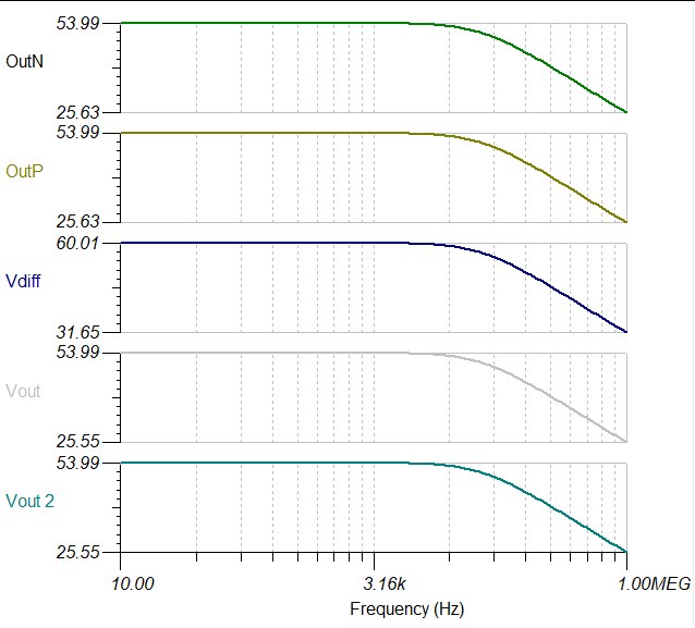
I am simulating a piezo transducer with capacitance of 66 nF and 100 K connected to this front end amplifier made for very low noise performance. The simulation results are horribly wrong. could anyone please let me know what is wrong in my simulation. Also I would like to calculate CMRR of this circuit from 10 Hz to 20 KHz. Please let me know. I intend to use it with gain of 10.

JFET_Frontendv2.TSC

Please let me know what is the issue?

  • Hi Sumeet, 

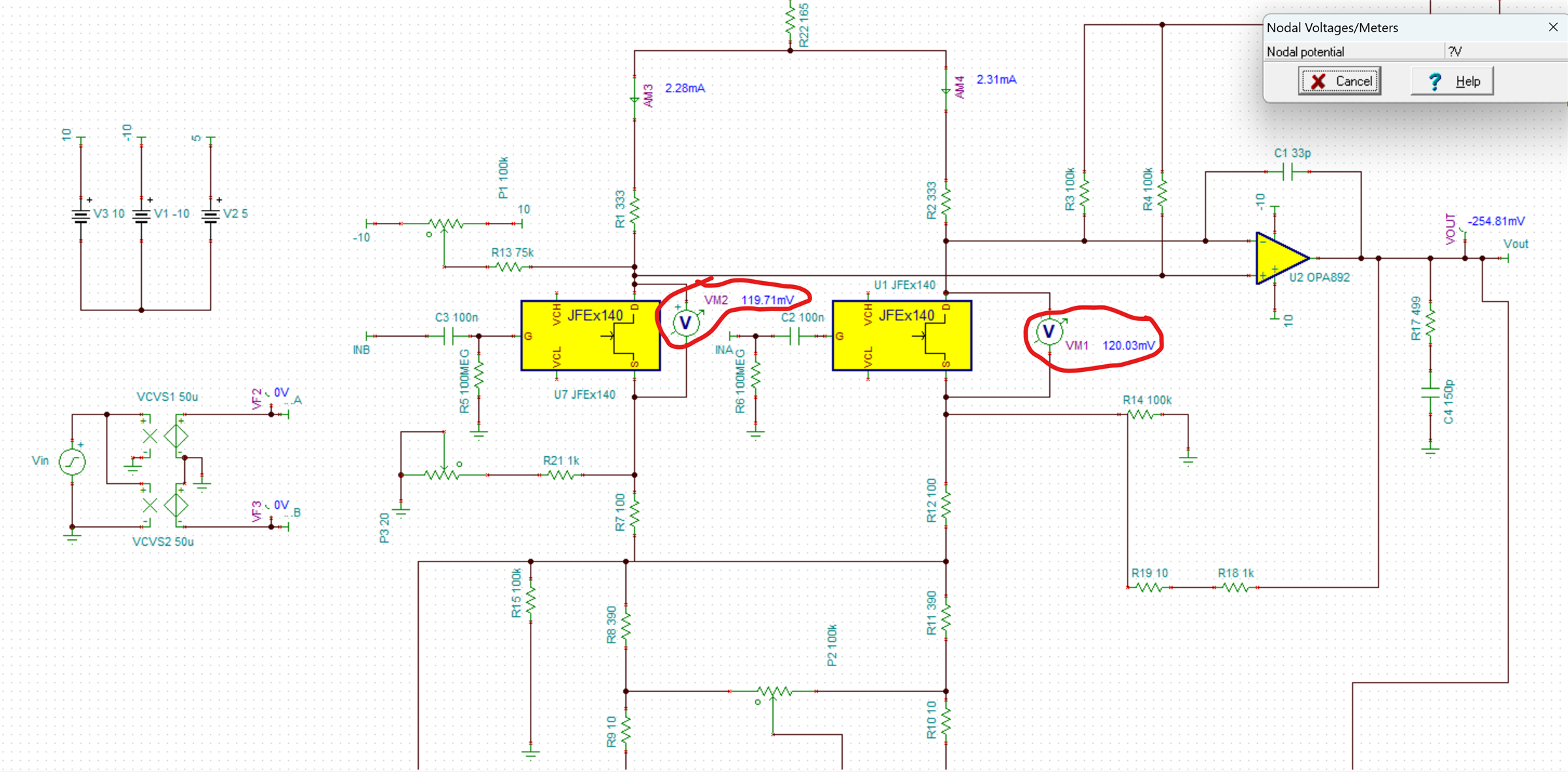
    My recommendation would be to significantly reduce the complexity of the circuit first for debug. All DC voltages within the circuit should be analyzed and valid before noise or AC analysis can be performed. There are a few issues with this circuit. Neither JFETs are operating in the linear operating range. You can see that the DC drain to source voltages show that the JFETs are operating in the triode region. Also the JFET on the right doesn't have a DC bias at the gate node. Capacitor C2 is DC blocking the bias voltage at the gate. 

    I wrote an application note for the JFE2140 with the feedback at the gate. In your circuit you have it at the source and I don't believe this will work. My app note covers the JFE2140EVM that I also built and tested. Do you need differential inputs? I don't  believe you will be able to achieve differential inputs with two JFETs and also have closed loop gain simultaneously. I have another circuit that can achieve differential inputs in a closed loop circuit however it requires 4 JFETs. 

    Here is my app note that covers the circuit I built and tested for the JFE2140EVM:

    https://www.ti.com/lit/an/sboa563/sboa563.pdf?ts=1729536126235&ref_url=https%253A%252F%252Fwww.ti.com%252Fproduct%252FJFE2140

    Best Regards, 

    Chris Featherstone

  • Chris, Don't want to hijack OP's thread, but I would be interested in seeing the 4 JFet Diff amp with close loop gain if feasible.  Thanks !

  • Hi Sumeet, 

    Chris is out of office for a week. He should be back on Nov. 4th. If this is urgent, please let us know. 

    Best,

    Raymond

  • I am working on it, will come back to you, Is there ref design with 4 JFET pairs in differential amplifier configuration.

  • Hello, 

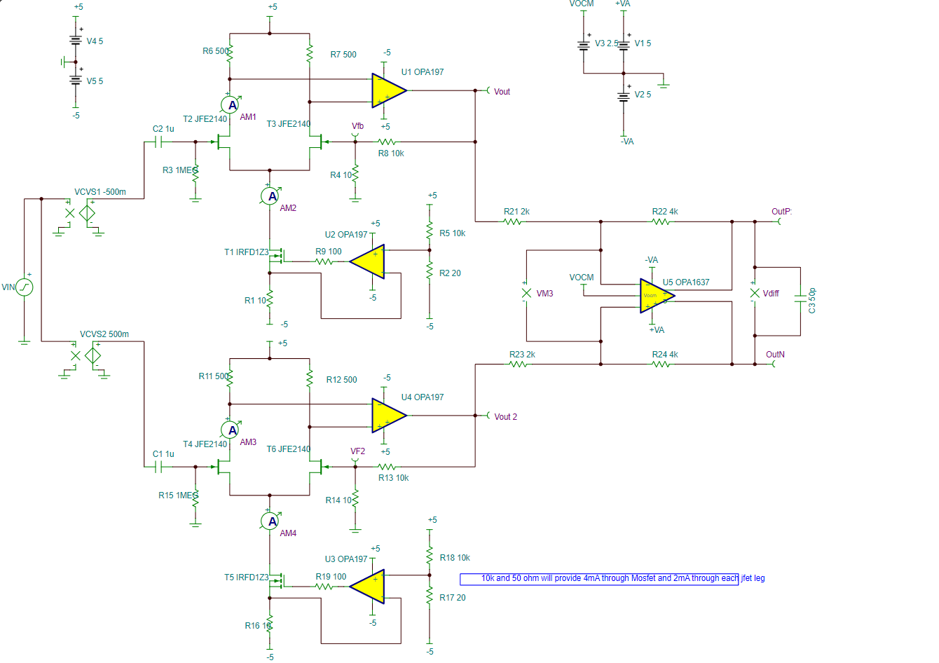
    Here is the fully differential solution with closed loop gain 

    Tina Simulation:

    JFE2140 and OPA1637 FDA.TSC

    Best Regards, 

    Chris Featherstone

  • Hey Scott, 

    No problem! My app note covers half the circuit (1 diff pair and composite amp). The theory applies here as well to understand the fully differential circuit. I just follow it up with the OPA1637. Here is the app note. 

    https://www.ti.com/lit/an/sboa563/sboa563.pdf?ts=1730925723713&ref_url=https%253A%252F%252Fwww.ti.com%252Fproduct%252FJFE2140

    Best Regards, 

    Chris Featherstone

  • Hi Chris,

    Do you have any simulation design that can achieve noise of 1nV/sqrtHz at 1Hz.

  • Hi Chris,

    Do you have any design that can achieve 1nV/sqrtHz at 1Hz.

  • Hi Sumeet,

    The lowest noise design I have is the JFE150 circuit below. 

    https://www.ti.com/lit/an/slpa018/slpa018.pdf?ts=1731086984591&ref_url=https%253A%252F%252Fwww.ti.com%252Fproduct%252FJFE150

    Best Regards, 
    Chris Featherstone

  • Hi Chris,

    1. Why did you switch from OPAx202 shown in the "JFE2140 Ultra-Low-Noise Preamplifier" AppNote, to the OPA197 for the 4-JFET close loop diff above ?  The AppNote seems to recommend a BiPolar OpAmp.  Perhaps it was just to accommodate a smaller voltage drop on the current sensing resistor, using the same OpAmps for both ? Also, would OPA1692 be a good/better choice for the OPAx202 shown in the AppNote ?

    2. With a gain of 1000x on the 4-JFET close loop diff above, if we have a 4mV Vgs offset mismatch on the T1/T2 JFE2140 jfets, won't that lead to a considerable DC bias offset on Vout ... possibly leading to clipping at the +/- 5V rails for large signal swings and/or a large DC component in the OPA1637 diff output ?   Perhaps the OPA197 feedback corrects for Vgs offsets, but I'm not seeing it at the moment.

    Thanks, Scott.

  • Hi Scott, 

    1. Why did you switch from OPAx202 shown in the "JFE2140 Ultra-Low-Noise Preamplifier" AppNote, to the OPA197 for the 4-JFET close loop diff above ?  The AppNote seems to recommend a BiPolar OpAmp.  Perhaps it was just to accommodate a smaller voltage drop on the current sensing resistor, using the same OpAmps for both ? Also, would OPA1692 be a good/better choice for the OPAx202 shown in the AppNote ?

    There wasn't any reason in particular. The OPA202 can be used as well. 

    2. With a gain of 1000x on the 4-JFET close loop diff above, if we have a 4mV Vgs offset mismatch on the T1/T2 JFE2140 jfets, won't that lead to a considerable DC bias offset on Vout ... possibly leading to clipping at the +/- 5V rails for large signal swings and/or a large DC component in the OPA1637 diff output ?   Perhaps the OPA197 feedback corrects for Vgs offsets, but I'm not seeing it at the moment.

    Yes the Vgs mismatch will get amplified and has the potential to be large if the mismatch is large. 

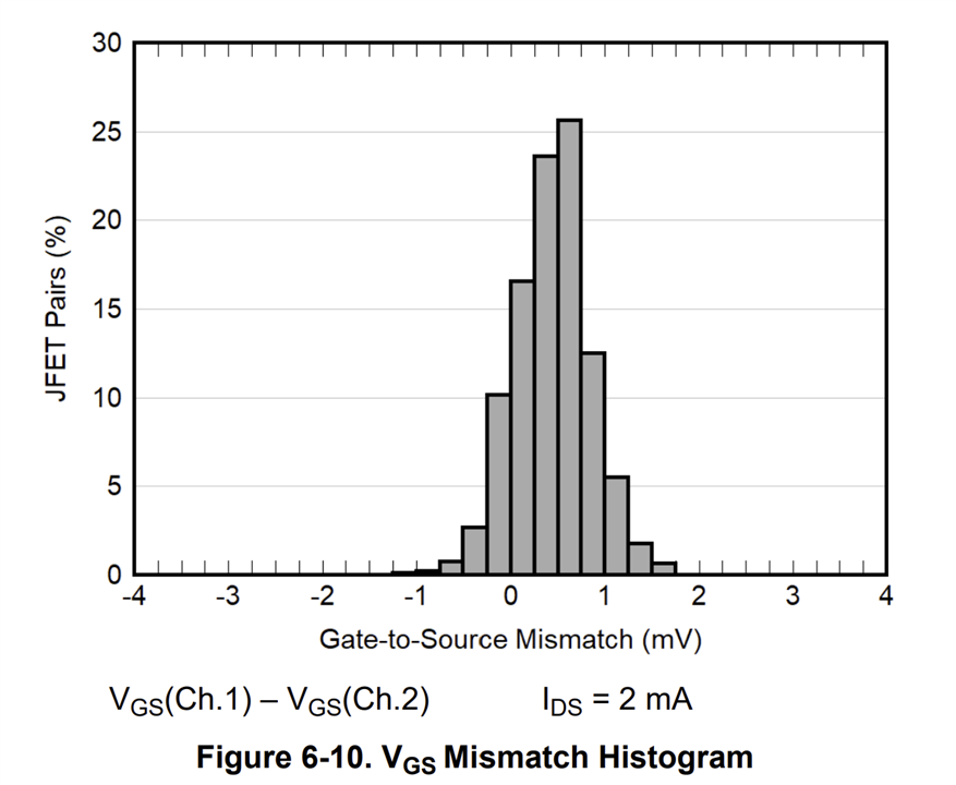
    The mismatch will on average be less than 1mV as shown below. 

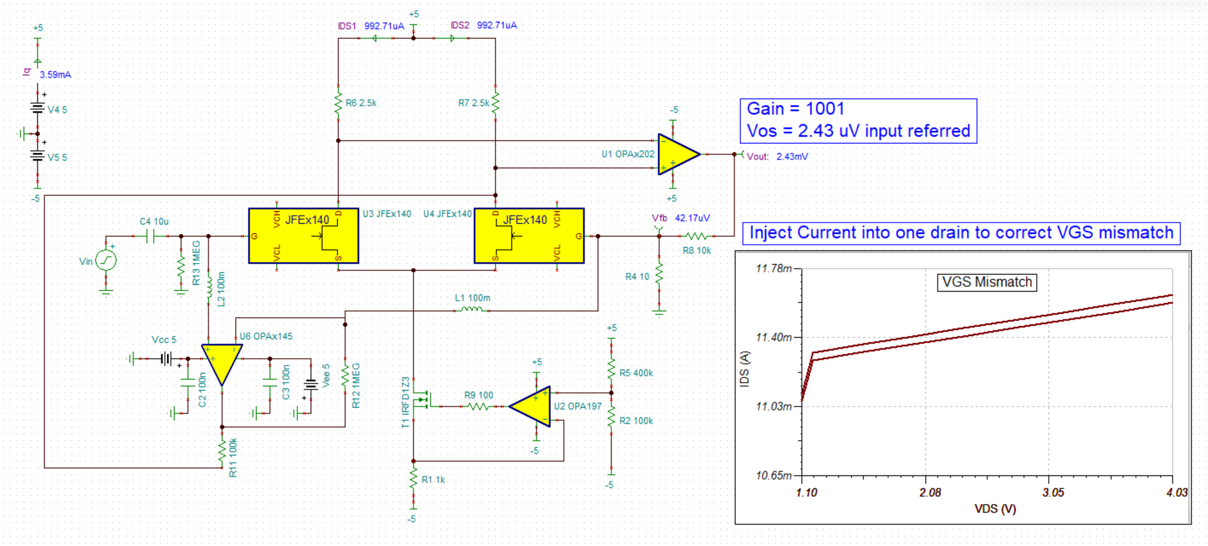
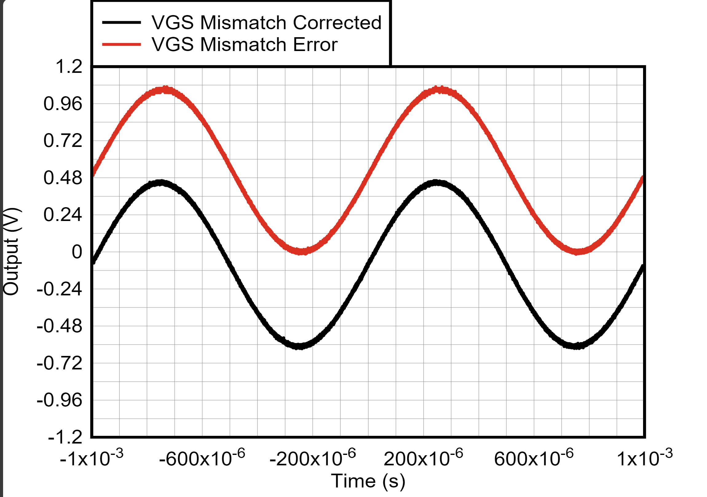
    If the mismatch is too large, an offset correction circuit could be used as I put on the EVM. I attached the tina simulation for the Vgs mismatch circuit below. I also bench tested the vgs mismatch circuit. You will inject the noise of the amplifier (OPA145) into the signal path however maybe it'll spark ideas for others to figure out a better way. Or it could just be an elaborate Rube Goldberg solution. Originally this circuit was written into my app note and I gave up on it because it seemed pointless specifically because of the noise injection. All the work is actually written into the app note and currently hidden. If it is found useful I may revise the app note and publish the work. The circuit is on the evaluation module that is released. 

    The VTO parameter in the model I made 2 mV higher for on JFET to adjust the mismatch.

    JFE2140 Vos Correction Circuit Cleaned up.TSC

    Bench measurement

    Best Regards,

    Chris Featherstone

  • If the LTspice simulations are to be believed, it looks like the v(inoise) of the differential amplifier can be reduced by about 1/3, but replacing the MOSFET constant current source by a BJT.  It seems like coupling a voltage reference with separate force/sense pins (e.g. REF3425) to a BJT would be a simple/elegant (?) way of doing this.  Since there is no PSpice model for the REF3425 :(, I tried it with the REF3212.  However, it seems like there is a major problem with the model, in that it ONLY works if the GROUND pin is actually grounded (i.e. 0 volts).  Is this topology/part a reasonable choice for the constant current source in the diff amp ?

    Thanks !

  • Hi,

    Chris, It would be great to have a 4 parallel pair of JFE2140, as it will reduce the noise. Chris can you help in doing that.

  • It will be worthwhile to see how 4 pairs of JFE works out in reducing the noise.

  • Sumeet,

    Chris is on vacation and will help out when he returns.

    Art

  • Do you know by when he will be available, I have some ideas which want to discuss with him as soon as possible.

  • Hi Sumeet, 

    It will be worthwhile to see how 4 pairs of JFE works out in reducing the noise.

    You may observe this in simulation. JFETs in parallel are known to reduce noise. This is observed in the datasheets between the JFE150 and JFE2140. The JFE150 has lower noise. The JFE150 is two JFETs in parallel. The JFE2140 is the same JFETs wired out for a matched dual pair. 

    Best Regards, 

    Chris Featherstone

  • Hi Chris,

    I checked the datasheet, it is only showing one JFET. I would like to use four matched JFE2140 pairs to make a ultra low noise differential amplifier. I would like to build it also to test it, but before that I want to simulate it and compare with some other parts. I am struggling to include the cascode connection in the design you had shared to reduce the input capacitance. Could we sync up on this to make this design work? As I said the volumes would be very large, if this design is cracked up.

  • Hi Chris, I have sent you a sim file, can you have a look at it please?

  • Hi Sumeet, 

    I have looked at the sim file and it is massive and will take time to go through. It also uses the incorrect model and not the released model that is available on the product page for the JFE2140. Please replace all the JFETs with the released model. 

    Best Regards. 

    Chris Featherstone

  • Hi Chris,

    I will do the same, meanwhile can you have a look at my design? Your suggestions would be very helpful.

  • Hi Sumeet, 

    The offset correction circuit that uses the OPA145 introduces the noise of the OPA145 into the signal path and the overall noise will be limited to the OPA145. For this reason I never published the offset correction circuit. 

    Please replace all the JFETs and provide the new simulation to me for review. Today will be our last day in the office and we will be out for two weeks. 

    Happy holidays. 

    Best Regards, 
    Chris Featherstone

  • Chris, best wishes for a GREAT holiday, for you and all your fellow TI folks !  Perhaps you could comment on using the REF3425 for the constant current source (above) when you return.  All the best, Scott.

  • Hi Chris,

    In the post above, you said: "I don't  believe you will be able to achieve differential inputs with two JFETs and also have closed loop gain simultaneously.".

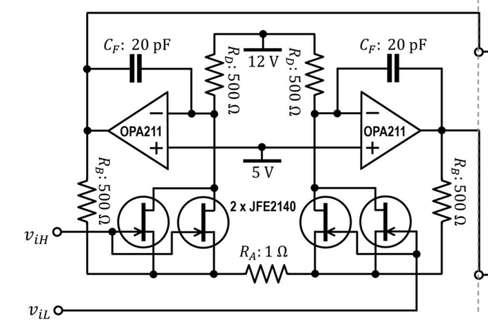
    I stumbled upon the circuit below, thoroughly described in:

    https://www.techrxiv.org/users/683672/articles/1008833-an-ultra-low-noise-fully-differential-amplifier?commit=245b27db9d01ba94ed9505da975636bb68f7ee4b

    IMHO, this is a very elegant implementation of differential inputs with closed loop gain.  The design uses four JFETs, but only as a means to achieve very low noise (0.9 nV/SrqtHz).  This could easily be converted to a differential input, two JFET design with closed loop gain and slightly higher noise.

    Best regards, Scott.

  • Hey Scott, 

    Cool find! I wonder if there are any tradeoffs with this solution. Looks like a promising design!

    Best Regards, 

    Chris Featherstone

  • I haven't been able to identify -any- downsides/tradeoffs.  One aspect I find particularly appealing/intriguing is that it always maintains a constant current through the JFETs even while amplifying (and as a result Vds variations are also quite small).

    As designed (for minimum noise), it draws significant current (7ma per JFET times 4), but the design can be adjusted to reduce this as necessary.

    If there is an inherent (DC) offset in the differential inputs (e.g. TDK ICS-40730 MEMS microphone), this gets amplified as well (at 1000x).  As such, I'd like to find a DC Servo circuit that doesn't add much noise ... absent that, some coupling capacitors are probably needed.

    In summary, for differential inputs and outputs, where a fixed close loop gain is desired, I think this topology is really hard to beat.

  • Hi Chris, I simulated the same design to see if I could get same noise level, apparently I am doing something wrong which I haven't been able to figure out, could you please have a look at it? I want to try this with 4 JFE2140s, but let me get this first one right. Could you suggest me positive temp coeff, tail current source? I want to offset the mismatch of negative coeff gm of JFE2140s with that constant current tail source, so that they find suitable operating points with variation in temperatures and, irrespective of the their mismatches and drain current. I have ordered JFE2140s, so once my sim circuit is good, I am actually going to build one based on that. I look forward to your support, hopefully, I am able to get this to production soon.

    7824.Noname.TSC

  • Hi Sumeet, 

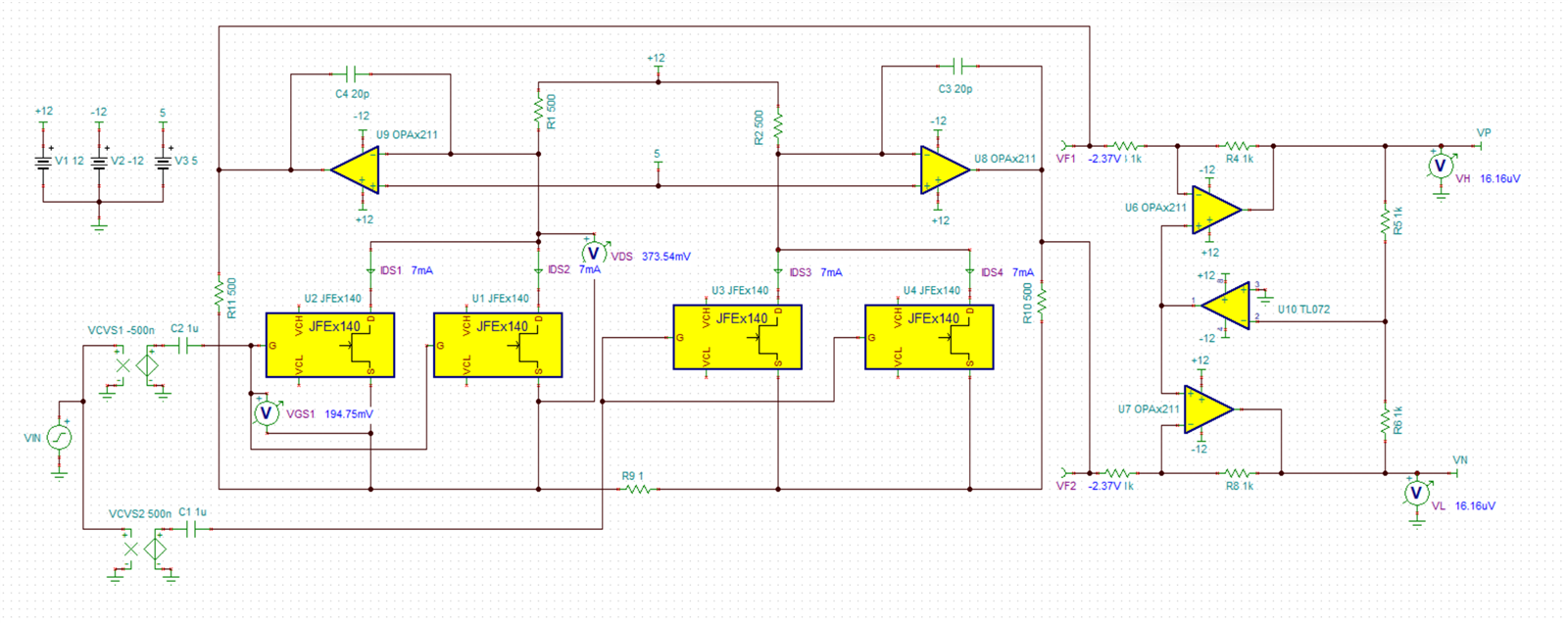
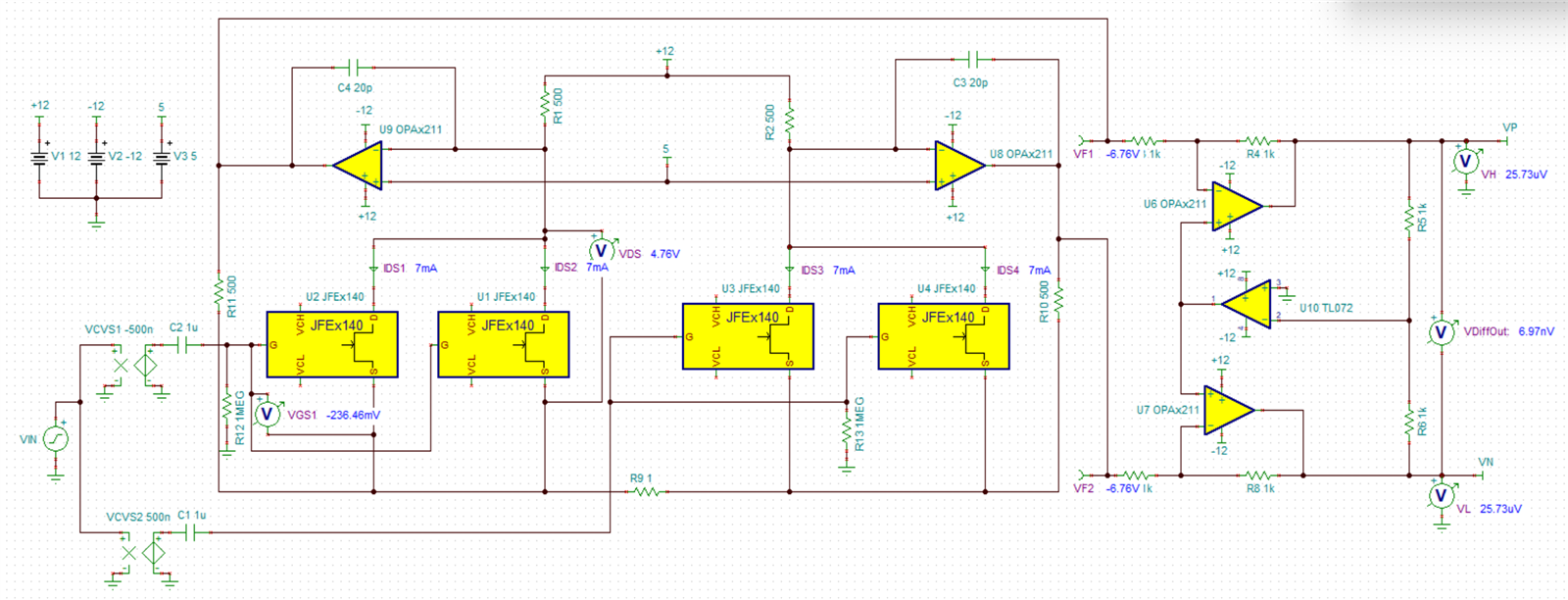
    I spent a significant amount of time consolidating the circuit down to fit on my monitor. I have attached the updated simulation. I ran out of time today to fully analyze the circuit. Can you look over the updated simulation to verify the connections you made? Currently there is not sufficient drain to source voltage on the JFETs to get them operating in the linear operating range. The VDS is 373.54mV. 

    For a current source you may consider this device:

    https://www.ti.com/lit/ds/symlink/lm134.pdf

    My team doesn't support the LM134 so a separate thread would need to be opened for that device. 

    Here is the new Tina simulation. Let me know if you find connection mistakes or if it looks good. 

    JFE2140 FDA.TSC

    There is no gate bias and this is probably one issue. I added gate bias as shown below to get the VDS to be in the linear operating range. 

    Best Regards, 

    Chris Featherstone

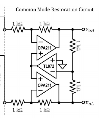
  • Chris, FWIW, I verified the schematic against the original article and it looks good.  Also, your VF1/2 levels match the CM bias that they were seeing in their tests.  I was able to reproduce the reported 0.9 nV/SqrtHz noise level in my LTspice simulations, although I did not include input coupling capacitors, nor the second stage "Common Mode Restoration Circuit".  Unfortunately, I've been unable to get Tina-TI running on my Linux workstation, so I will be interested to hear your findings. Thanks !

  • Sumeet, the results from my LTspice simulation of this circuit are posted below in case  they are helpful to you.  This is without the input coupling capacitors and the second stage "Common Mode Restoration Stage", which should not substantially affect the v(inoise) results.

    +2/-2mV sinewave in, +2/-2V sinewave out, THD 0.0005%

    With two JFETs on each side (original circuit): 1kHz 0.874, 100Hz 0.895, 10Hz 1.078, 1Hz 2.185, all in nV/SqrtHz

    With four JFETs on each side (see below): 1kHz 0.622, 100Hz 0.637, 10Hz 0.775, 1Hz 1.593, all in nV/SqrtHz

    With four JFETs on each side, all -five- resistors in the circuit are cut in half, -and- the two capacitors are doubled.

    ALSO, with four JFETs on each side, the OpAmps (and resistors) are moving a lot of current.  I have not investigated whether the OpAmps are indeed able to perform as simulated.

    Best regards, Scott.

  • Hi Scott,

    Thank you Scott for sharing your sim result, Those results looks very good, Do you have LTspice model of JFET2140, which if you can share it with me? That would be very helpful. How did you connect the tail of all four on each side?

  • Sumeet,  I am just using the (unmodified) JFEx140 PSpice model as downloaded from the JFE2140 product page on the TI website (along with an auto-generated symbol).  I would be happy to share them, but haven't yet figured out how to upload non-image files to the forum (perhaps I need more Prodigy points ?).  As to the tail connection, I have all four JFETs on each side "fully" in parallel with all four sources connected directly together.  As I stated earlier, cut the resistors (500 ohm, 1 ohm) in half to maintain the 7ma through each JFET, and double the caps to compensate for the lowered resistance.

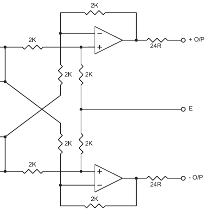
  • Sumeet, Also ... in the circuit Chris shows above (which I assume you supplied) it looks like the Common Mode Restoration Circuit from the original article.

    I'm not aware of your goals/requirements, but you might want to consider replacing that circuit with the "Double Balanced" circuit shown below.  Uses one less OpAmp, provides additional gain, and may have better CMRR.  Best regards, Scott.

  • Hi Scott, thanks for your reply, I will try out your suggestion, and will keep you posted.

  • Hi Chris,

    This are questions for you:

    1) IG input gate current spec given in datasheet is actually the gate to source leakage current (IGSS)? Is it at max 10 pA.

    2) What would be Gm and VGS spread for say a 1000 pieces? The DS only mentions spread of 5 pieces. It is very much vital for my application to know probable spread of this parameters?

  • Hi Scott, Is possible for you to send me LTspice model of JFE2140?

  • The forum seems picky on which type of files can be attached.  I renamed my JFEx140.asy to JFEx140.asy.txt to allow attachment.  I use the ASY file as the symbol and then the jfex140.lib as the model with the LTspice statement ".include jfex140.lib".

    JFEx140.asy.txt
    Version 4
    SymbolType BLOCK
    RECTANGLE Normal -48 -56 48 56
    WINDOW 0 0 -56 Bottom 2
    WINDOW 3 0 56 Top 2
    SYMATTR Prefix X
    SYMATTR Value JFEx140
    SYMATTR ModelFile jfex140.lib
    PIN 48 -32 RIGHT 8
    PINATTR PinName D
    PINATTR SpiceOrder 1
    PIN -48 0 LEFT 8
    PINATTR PinName G
    PINATTR SpiceOrder 2
    PIN 48 32 RIGHT 8
    PINATTR PinName S
    PINATTR SpiceOrder 3
    PIN -48 -32 LEFT 8
    PINATTR PinName VCH
    PINATTR SpiceOrder 4
    PIN -48 32 LEFT 8
    PINATTR PinName VCL
    PINATTR SpiceOrder 5
    

    jfex140.lib