This thread has been locked.

If you have a related question, please click the "Ask a related question" button in the top right corner. The newly created question will be automatically linked to this question.

OPA323: Pspice file for OPA323 is not showing results as intended.

Part Number: OPA323

Tool/software:

Hello 

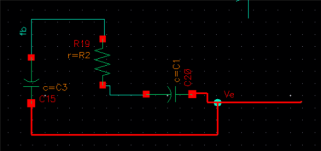
I am using Pspice .lib file as a circuit model in Cadence for using it in a type III compensation system I use the model as it is but I feel there is a lot of extraneous code in the pspice model file.
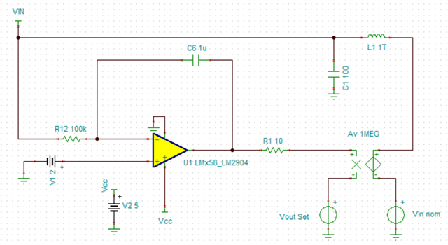
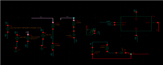
For the following circuit: 


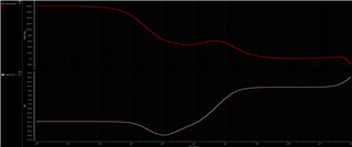
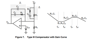
I am expecting a response as this:


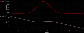
The above response is typical for a type III compensator with phase boosting

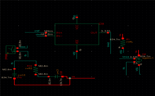
As soon as I insert the OPA323 model:


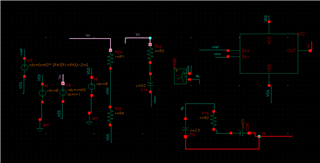
I get a very unexpected open loop gain and phase plot with both the phase and the gain starting from a negative valued scale:


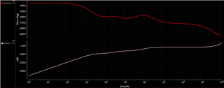
Is the code for the pspice model correct. WHat needs to be done or edited in it. I just need to use the OPAMP as it is and then compensate it using my values

  • Hello Usa,

    Try suppling power to the op amp. I see that power is 0V.

  • So Ron,
    The phase plott now is expected, however. it does not give me a much bigger phase boost as I was expecting, however, the gain still starts from a negative axis.


    Hoping to hear from you soon, is there anything in the code itself that may be an issue?

  • Usa,

    Can you show the updated circuit? Ideally with the pieces connected with wires like a normal op amp circuit. 

    Nevertheless, the problem likely lies here. There is no DC feedback.

    You need something like below (the stuff on the right side) to get a DC operating point without 'any' AC feedback. This method keeps circuit effectively open loop. See how I get a closed loop for DC, but not AC.   

  • Hi Ron
    So I just need to put the OPAMP OPA323 in place of the block in figure 7 shown in the following document of TI below:
    https://www.ti.com/lit/an/slva662/slva662.pdf?ts=1716191717178

    This should be pretty straight forward,I have the DC bias set up for both the inputs:

    There is no closed loop here, I need the ac gain and phase plot from Vo to Ve, meaning A(s) OPENLOOP = Ve/Vo 

  • Essentially My circuit is as it shows:

  • Usa,

    The simulations won't give a AC gain until it can resolve a DC operating point. You can connect your Ve to my Av gain block (lower gains work too). Set "Vout Set" to equal the nominal DC value for Ve.  Optional is to set "Vin Nom" to nominal value for Vo.  After my LC filter connect to your Vo.

    Run a DC sim to verify that Ve servos to the target value and Vo should be close to nominal voltage. You can inject AC into bottom side of my C1 cap (shows up on Vo). Then you can read Ve. That is your Ve/Vo gain 

  • 1. So Essentially what you are trying to say is that I need a VCVS at the output of the OPAMP and externally Bias it with a DC operating point like shown in the figure plot below when I have to simulate the AC characteristics of the OPAMP? Where Vmid is the output of the OPAMP, Vb is bias voltage (VCC/2), and Ve is the final voltage that feeds back to the input through some compensation passives:

    The Output should be DC biased as in? 

    2. But will this also be needed if there is a load connected to the OPAMP (like the resistor in my case)? I have this OPAMP in a bigger loop connected to three comparators. How will the DC bias of the output be set in that case? I am just wanting the Ve to give me different values across the VCC range depending on my common mode input bias. Kindly suggest