


Part Number: UCC25600
Tool/software:
Hi Team,
My customer was confused by the typical application circuit vs the reference design schematic. Can you maybe change the datasheet here.
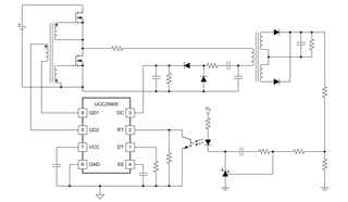
and
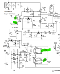
I discussed it with the Power Design Team and got the following explanation:
There are LLC controllers in our portfolio who need to have both gate driver outputs assigned correctly, because when they start they need to charge the bootstrap capacitor (therefore low side FET starts first) that supplies the high side HV gate driver.
For the UCC25600 it’s not the case, because there is no bootstrap to charge and a simple gate drive transformer is driven, so in theory as the controller starts switching, it’s not important which FET starts first. Also, in overcurrent protection or other protections (UVLO, OV, OC and TSD, see block diagram), both FETs are driven low by means of two AND gates, which are disabled at the same time.
Anyway, for the sake of avoiding confusion and from my perspective, GD1 should drive the high side FET. That means the typical application diagram on first page of UCC25600 DS is not correct. In fact, when GD1 is on, there is a positive potential applied to the non-dot of gate drive transformer. That means the high side FET’s gate has the positive on the non-dot, which means there is a negative potential on the dot of the transformer on high side FET.
Now, referring to figure 8-8 (typical application schematic), this is correct because it’s not important that a dot or non-dot is applied to the gate but only that the transformed voltage is applied with the right polarity: example….GD1 is high, then OUTA is high, a positive potential is applied to pin 4 of T3 (non-dot), while OUTB = 0. Now a positive voltage is applied on both non-dot outputs of T3 (pins 5 and 7)….that means a positive voltage is applied to the gate of Q1 (high side FET)….I hope it’s now a bit more clear
Thanks
Jan
