This thread has been locked.

If you have a related question, please click the "Ask a related question" button in the top right corner. The newly created question will be automatically linked to this question.

INA333: 96Hz sine noise without input

Part Number: INA333

Tool/software:

Hi,

I've an issue that I cannot solve on the simple pcb I designed and I attach to the post. It's an amplifier board for a mems microphone, but, even without any input and the microphone pcb disconnected, I have a 96kHz perfect sinusoidal noise of about 10mV rms. When I replicate the same board on a tht board and without LDOs I don't have the issue. I tried adding a resistor in serie on the output, another low pass just before the acquisition, etc, but nothing changed. 

Is it a ground loop? It's my first pcb, so it's difficult for me to visually identify it, so I attach a schematic of the pcb too. 

The connection to the acquisition board is made with a micro USB B, I know it's not designed for analog signals, but I need a cheap and small connection for a lot of cables, I hope this is not the issue.

ampli: INA333AIDGKR

LDOs: TPS76325QDBVRG4Q1 and TPS72325DBVR

  • Hello Giovanni,

    When I replicate the same board on a tht board and without LDOs I don't have the issue.

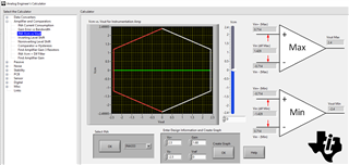
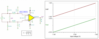
    This is linear operating range of your INA333 configuration. 

    Here is the simulation:

    0317.INA333 Current Sensing 09252024.TSC

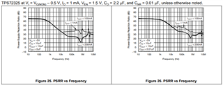
    My guess is that the 96kHz noise is likely coupled through your LDOs from USB port. Your LDOs do not have adequate PSRR to filter out the 100kHz switching noise and INA333 is also ineffective to attenuate 100kHz noise. 

    LDOs: TPS76325QDBVRG4Q1 and TPS72325DBVR

    For LDOs, the PSRR will be no better than 20dB at 100kHz. So 100kHz switching noise will be attenuated significantly. 

    One way is to filter out ripple noises from +/-2.5Vdc or  +/-5Vdc rails. You can try dual RC filters to get rid of switching noise. 

    RC Ripple Noise Filter 10292024.TSC

    Or find some low ESR MLCC 10uF capacitors and placed in the following nodes. 

    Please let me know if this solve your issues. 

    BTW, you may need to place differential and common mode filters in front of INA333 IA. 

    If you have other questions, please let me know. 

    Best,

    Raymond

  • Hello Giovanni,

    Please check out our LM2776, positive to negative rail charge pump. Vcc is lower noise USB regulator. So you should use Vcc rail to generate -2.5Vdc or similar. 

    You can also use 5Vdc to drive INA333, but the you need to alter the circuit a bit (since you already have the PCB).  

    https://www.ti.com/lit/ta/sszt970/sszt970.pdf?ts=1730208766996

    If you have other questions, please let me know. 

    Best,

    Raymond

  • Hello, thanks for the tips, here's a summary of what I tried so far.

    • C2 and C3 are already low ESR caps, as well as C7 and C1. A low pass as shown in light blue in your picture actually increases the noise level by introducing new modes.
    • If I remove R1, R2, C8 and C9 I get less noise, but still a peak in the fft. 
    • If I completely remove the USB connector and I connect supply and output via wires, I completely delete the noise. So yes, somehow the noise comes from the USB receptacle interaction with the PCB. 
    • I scratched the tracks of the +-5V to disconnect them from the USB connector and I connected them via wire. However, with the USB receptacle in place and the ouput and GND connected via USB cable the noise persisted. 

    I tell you some more details to explain the design and ask you what I can modify, if I have to, in the receptacle choice. 

    I used an USB B because I need something small (10mm max) and cheap that I can connect via cheap shielded cables. The USB or jacks cables are perfect for that, but they are not the standard. If I use the positive to negative charge pump as you suggest I can have a 3 pin connector, which increase the number of available choices I imagine.

    Is there a more standard choice in analog devices which is small, cheap, shielded and robust?

    Last thing: I have some PCBs that I can test so it's not a big deal if I need to sacrifice some of them by scratching etc.

    Best, 

    Giovanni 

  • Hi Giovanni,

    Please make the +2.5Vdc and -2.5Vdc ripple voltage to the INA333 IAs and let me know. That is your noise source for the design. Your +/-2.5Vdc sources should have ripple noise in a few mV in amplitude, and low frequency noise.  

    To attenuate the switching noises from USB power, you need to place LPF filter (-20dB/dec) at < 100Hz. Prefer to have -40dB/dec roll off in your RC filters. 

    Your low ESR cap is not low enough. You may need to use MLCC with ESR <2-5mΩ range + RC filter before the charge pump's supply rail, may be even after depending on the ripple voltage amplitude. 

    Terminate your analog GND to a known GND or earth GND, not "floating" GND. 

    Please get me these data and I will try to figure it out how to improve the design. 

    Best,

    Raymond

  • Hi Giovanni,

    I assume that your issues are resolved. I am going to close this query. 

    If you have other questions, please let us know. 

    Best,

    Raymond

  • Hi Raymond,

    I assembled more PCBs with the same design and apparently the amplitude of the noise depends on the soldering. The peak always appears at around 96-100kHz, but with a cleaner soldering process I can decrease and broad the noise. 

    Anyway, because the noise is decreased to the order of 50uV, I'll keep the design like this. 

    I'll try the design with the charge pump next and I'll let you know. With this design, I can use a 3 pin connector like a jack 3.5mm; is it better for an analog signal?

    Regards,

    Giovanni 

  • Hi Giovanni,

    I assembled more PCBs with the same design and apparently the amplitude of the noise depends on the soldering.

    This looks like this may be soldering issue also. Please clean the PCB after the soldering is completed. We use ultrasonic bath to clean these PCB board. For home, use soap and water and soft tipped toothbrush to clean the surface, and dry it in an open air or blow the excessive water out with a low pressured compressed air. 

    I'll try the design with the charge pump next and I'll let you know. With this design, I can use a 3 pin connector like a jack 3.5mm; is it better for an analog signal?

    The charge pump is better alternative. D- node is a digital switching node, and contains much switching harmonic noises. Even with charge pump, you still need to watch out for the coupled switching noise. Use LPF and low ESR cap to get rid of ripple noises.

    If you have other questions, please let us know. 

    Best,

    Raymond