Other Parts Discussed in Thread: THS4551, THS4505
Tool/software:
Dear Specialists,
My customer is considering THS4151 and has a confirmation request.
I would be grateful if you could advise.
---
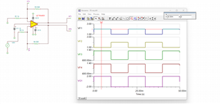
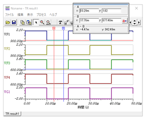
When ±2V is input to VIN_P and VIN_N is fixed at 0V
Input resistance is 1kohm and the feedback resistance is 500ohm.
VOCM = 1.5V,
the output voltage will be as follows.
VOUT_P = 2V@VIN_P=2V
=1V@VIN_P=-2V
VOUT_N = 1V@VIN_P=2V
=2V@VIN_P=-2V
A negative voltage is input to VIN_P, but the voltage VP applied directly to the + terminal
will be 0.67V~1.33V.
VN is the same voltage, 0.67~1.33V.
TINA TI simulation went well.
On the other hand,
The common mode input voltage range of the THS4151 is (Vs-) +1.5V to (Vs+) -1.5V.
When used with a single +5V power supply, it becomes 1.5V to 3.5V.
Does this mean that it cannot be used because it is outside the input voltage range?
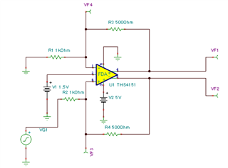
THS4151 Application Circuit.TSC
ーーー
I appreciate your great help in advance.
Best regards,
Shinichi