This thread has been locked.

If you have a related question, please click the "Ask a related question" button in the top right corner. The newly created question will be automatically linked to this question.

VCA810: VCA810 Log Amplifier

Part Number: VCA810

Tool/software:

Hello,

I have a question concerning the VCA810 Wideband and Variable Gain Amplifier that I use as a Log Amplifier from -40dB to 40dB gain.

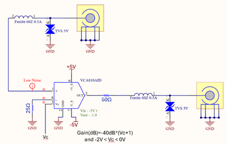
According to the datasheet, the component has an VOLTAGE_OUTPUT_SWING = +/-1.8V (3.6Vpp) for Vc=-2V and RL=100Ohms.

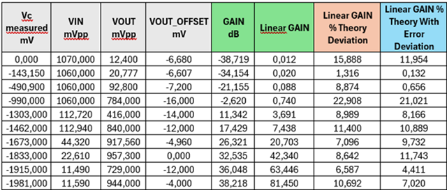
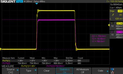
I control 10 different gains thanks to Vc from -2V to 0V, and for every gain test, I am almost at +/-1.7V, which is suitable. But for my X1 gain, I have poor results. The ouput is limited and +/-1.1V...So almost 600mV away of the real limit. As in Figure 1 bellow, for VIN=1.80V (yellow), VOUT=1.05V (purple). 


FIGURE 1

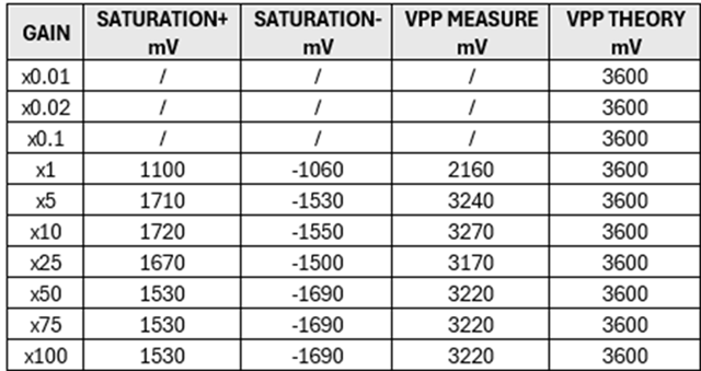
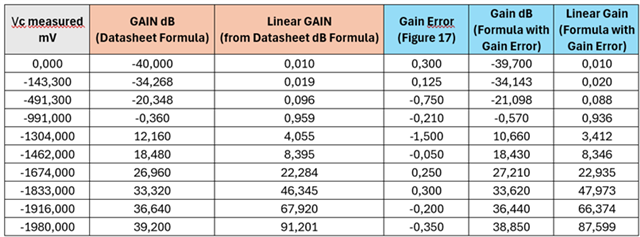
The other probleme is for the gain accuracy. Except for gain X1, for every gain, the output saturation is at almost +/-1.8V, but the gain is not very accurate, for acheiving 1.8V at the ouput for a we need more than 180mV for gain X10, more than 18mV for gainX100, etc. For example, if my VIN=1.8VPP, I have differente results if my signal is centered according to 0 or if it is between 0V and 1.8V as we can see in Figure 2 and Figure 3 : 

FIGURE 2                                                                                     FIGURE 3

Indeed, this is due to an "early limit" in the output swing I guess. But this means that the gain is only accurate bellow a certain value of VIN (under 500mV for example)...

Some theories are suitable then : 

  • For the limit problem at +/-1.1V for gainX1 : maybe the teeple point? Vc control unstability?
  • For the gain accuracy : same limit output swing problem?

I have a 25Ohms resistance at Vc pin to the ground, a 50Ohms resistance in series at the ouput pin to adapt.

Thank you for your help.

Best regards.

  • Hello José,

      Thank you for the details! Would you be able to share a snippet of the schematic with us? And, I had a few more clarifying questions:

    1. What is the Vc, or Vc range, you used to measure at a gain of X1 (1V/V) for the first scope shot
    2. When mentioned gain accuracy, is 180mV and 18mV more referring to the input Vin level or the Vc bias level? I think based on your next sentence you are referring to input Vin level at each gain is different and not consistent in terms of ratios?
    3. Are these plots being taken in consideration for Vc and gain error in relation to Vc?


      It might be easier if you can put columns: Vc vs Input Voltage vs Gain in a table for each measurement that you were able to conduct during your testing.   

    Thank you!
    Sima

  • Hello Sima,

    Thank you very much for your answer!

    First of all, yes, here I have the schematic around the VCA810 (Figure 1) :

    FIGURE 1 : SCHEMATIC

    I have my source at 50Ω, PIN_1 (V+) at High Impedance, PIN_5 (OUT) at 50Ω and the Oscilloscope at 1MΩ. Also, the resistance at PIN_8 (V-) was at 10Ω before, I changed it with a 25Ω but there is visibly no changes in the performance.

    Answering in order to your questions :

    1. For my gain of X1 (1V/V), my measured Vc is equal to -990mV.
    2. Yes I am referring to the input Vin level, meaning that my signal does 180mV or 18mV peak to peak and not a Bias signal. Yes the gain is not consistent in terms of ratios.
    3. I just took in consideration the plots you sent and I am working with -2V < Vc < 0, so there is no problem concerning FIGURE 6. You will find a table of my limited VOUT Swing, a VC vs input Voltage vs Gain Table with the theory and the measurements, with and without the gain error consideration. 

    First the output voltage swing : 

    FIGURE 2 : OUTPUT VOLTAGE SWING

    I really think the problem is related to my Output Voltage Swing limitation rather than the gain error itself…Even if I am limited to the values in Figure 2, my gain is really “damaged” before reaching them.

    Then I measured Vc control voltages and calculated the gain that we see in Figure 3 that gives is the theoretical values for linear and dB gains with the datasheet formula :

    And also thanks to the FIGURE 17 of the datasheet, I introduced the error :

    FIGURE 3 : THEORETICAL GAIN WITH ACTUAL Vc MEASUREMENTS AND ERROR GAIN

    For my tests, I used a square signal at 100kHz frequency, changing the amplitude to be able to see coherent signal according to the swing (Figure 4). 

    FIGURE 4 : GAIN MEASUREMENTS AND ERROR GAIN

    In Figure 4, we have the results and the percentage of deviation of the measured linear gain against the theoretical gain and theoretical including error gain. We can see that for X1 gain, we have the highest deviation at 21%... (Figure 5)

    FIGURE 5 : X1 GAIN

    To resume, the output voltage swing is limited before +1.8V and -1.8V that maybe causes a gain problem at some levels even if this one is not perfect. Knowing that for small entry and centered around 0, signal it works better. The problem also remains that I really need all the positive output voltage swing range.

    Thank you for your help,

    Best regards.

  • Hello,

    I read other conversations around this component, they had a similar problem, I would like to know if there is another reference maybe capable of doing different gains? Or if it comes from the schematic? 

    Thank you.

  • Hello José,

      I apologize for a delay getting back to you. I was on out last week, will be able to review this in-depth and get back to you by tomorrow.

    Thank you for all this in-depth testing and your patience!
    Sima 

  • Hello Sima,

    No problem, I look forward to your response and will give it my full attention. Thank you very much for your help.

    Best regards.

  • Hello José,

      Thank you so much for your patience. I was looking over this device in depth, and this device does have varying output voltages depending on gain setting.

       Comparing to your table, Figure 1, from your testing it doesn't really follow this graph, and you are not reaching the expected 3.6Vpp closer to the 40dB gain. Would you be able to quickly test some of these points without the ferrite bead to see if we get closer to these values. Overall, this device does have varying max output voltages depending on the set gain. 

       The other Figures were very helpful, especially inclusion of the gain error vs normal theory equations. This device should follow closer to the gain in dB, but we have other devices similar to this device that is linear (V/V) gain control if that is what you need for your application. The note on the drastic error at 0dB is important. When switching between attenuation to gain, it seems to be switching between different blocks within the amplifier which leads to a larger error at the 0dB mark: 

      As an example (analogy) of what might be happening: we sometimes see this in amplifiers that introduces error in the crossover region in rail-to-rail amplifiers, which in those types of technologies is solved via zero crossover topology to eliminate higher offset voltages at a certain crossover input common-mode voltage:

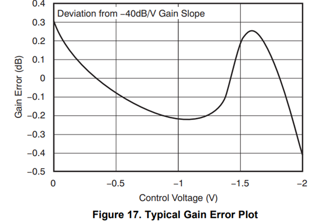
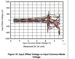
      (example from different device)
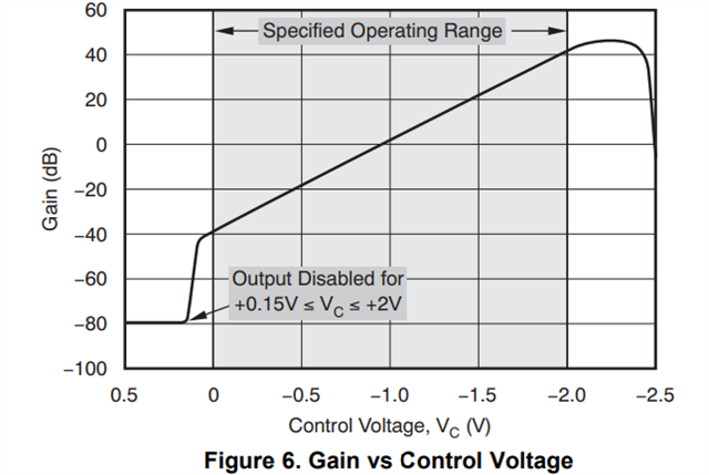
      Is output voltage consistency in terms of saturation important for your device? I will be able to look at our portfolio to see if we can suggest a different device. 

    Thank you again for all the testing and your patience on this issue,

    Sima