Because of the holidays, TI E2E™ design support forum responses will be delayed from Dec. 25 through Jan. 2. Thank you for your patience.

This thread has been locked.

If you have a related question, please click the "Ask a related question" button in the top right corner. The newly created question will be automatically linked to this question.

INA186-Q1: Short to GND at IN+, IN-

Part Number: INA186-Q1
Other Parts Discussed in Thread: INA186

Tool/software:

Hi team, 

Customer have a special test case for INA186-Q1 that would damage device. Would like to get some suggestions from your side. 

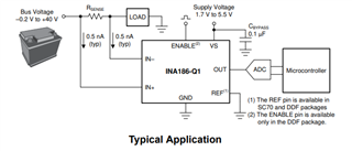
Take below block diagram as example, the test case is that VS and GND pin will be floated and then short IN- & IN+ to GND. Customer found INA186-Q1 was damaged after this test. The voltage they measured at VS and GND is about 13V. So IN+ & IN- are about -13V at this case. It is out of the ABS value in datasheet. 

But this test case is required. So do you have any recommendations that INA186-Q1 can survive from this test? Or any other device can work? 

Some thoughts from my side, please help check and let me know your thoughts. 

1. Add a current limiting resistor at both IN+ and IN-. To avoid the reverse current out of INA186 spec. But how to select the resistor value? 

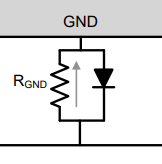
2. Add a reverse protection circuit as below, this is an example from our high side switch product. 
Thanks!

Ethan Wen

  • Hey Ethan,

    I may need little more information, but in general it is not a good idea to float device ground pin. We mostly assume that device's ground pin is always connected to board ground. Floating GND and then connecting while input voltages are present can create latch up conditions.

    1. You want to limit input current (current flowing into/out of input pins) to <5mA at any point. Conservative calculation for Rprotect is just > Vin/5mA.

    2. Yes you need to ensure that GND pin voltage does not exceed Vs voltage by 0.3V according to Absolute Maximum Datasheet ratings table.

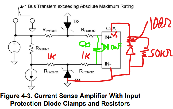
    Possible protection circuit can look like below. Rprotect1 limits current into clamping diodes to prevent excess power dissipation. Rprotect2 limits the input current into device pins. Although Rprotect2 will limit device input current to Vf_D1/Rprotect2, so they may not need to be as high as 1kOhm.

    I put a diode from VS pin to GND pin to clamp this differential voltage to < 1 diode forward voltage drop, although since this is usually greater than 0.3V, I also have a current limiting resistor (10-Ohm) but may need to higher to limit current to < 5mA. I also have a 50kOhm resistor in parallel to help keep this voltage stable during transitions from floating to connecting Vs/GND pins. 

    The nice thing about the INA186 is that it is high-input impedance and can operate with input resistor (up to 2kOhm) with minimal affects on accuracy as long as you can provide a >10nF differential capacitor at input pins (see green capacitor above). See this document for more information and data on device with high input resistors.

    https://www.ti.com/lit/ug/slya042/slya042.pdf

    Best,

    Peter

    Sincerely,

    Peter

  • Hi Peter, 

    Thanks for your detailed explanation.

    Further more, we want to check with you how this device be damaged at this test. Customer measured 13V on both VS and GND pin to a reference ground. IN+ and IN- is about 0V to this reference ground. Do you think the damage is happened at the path between GND and IN+/IN-? 

    You mentioned the input current (current flowing into/out of input pins) should be limit to <5mA at any point. Can I understand that if current flow into/out from IN+/IN- to GND >5mA may cause damage on it? 

    Regards,

    Ethan Wen

  • Hey Chuqiang, 

    The voltages described is a violation of the Absolute Maximum Vcm rating of IN-to-GND > -0.3V. If input is 0V, and GND is 13V, this is a Vcm of -13V, which will absolutely break the device with a pathway in between GND pin an IN+/IN-, yes.

    When these voltage violation happen, ESD cells or their body diodes will become forward biased and start conducting high currents for sustained periods of time (>500ns). This is all it takes for the ESD cell to become extremely heated and burn or causing burn damage elsewhere in the device. But if this forward bias current is limited to <5mA, then excessive heat (and damage) can be avoided.

    Sincerely,

    Peter