This thread has been locked.

If you have a related question, please click the "Ask a related question" button in the top right corner. The newly created question will be automatically linked to this question.

OPA2333-Q1: input impedance in full temp

Part Number: OPA2333-Q1

Tool/software:

Hi Team,

I would like to check the V+ input impendance in full temp. May you let me know the value or histogram?

Regards,
Roy

  • Hello Roy,

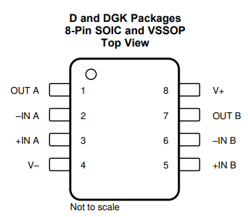
    Do you mean the V+ pin in this diagram? Below is the answer, but I doubt I understood the question correctly. 

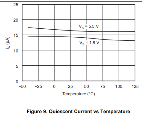
    There are these ECX table spec limit

    IQ doesn't move much with temperature.

  • Roy,

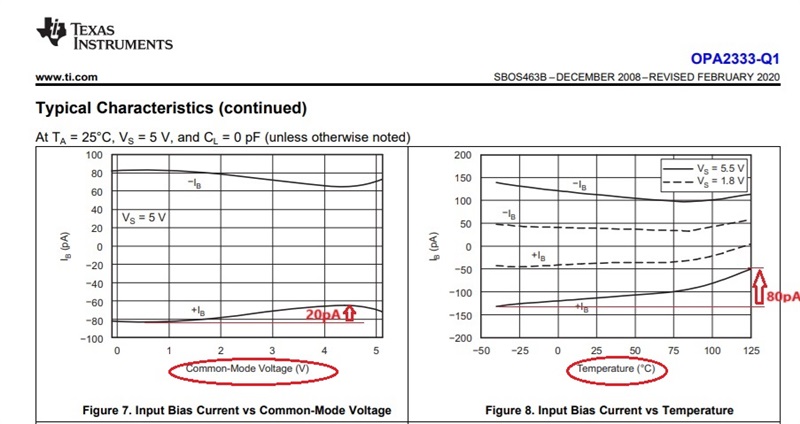
    I believe you might be referring to the input common-mode impedance and if so this may be calculated using IB vs Vcm and IB vs Temp graphs - see below.

    Even if you assume the worst case that there is correlation between IB variation due to Vcm and Temp, you may calculate Rin_cm=5V/100pA = 50Gohm.

  • Hi Marek,

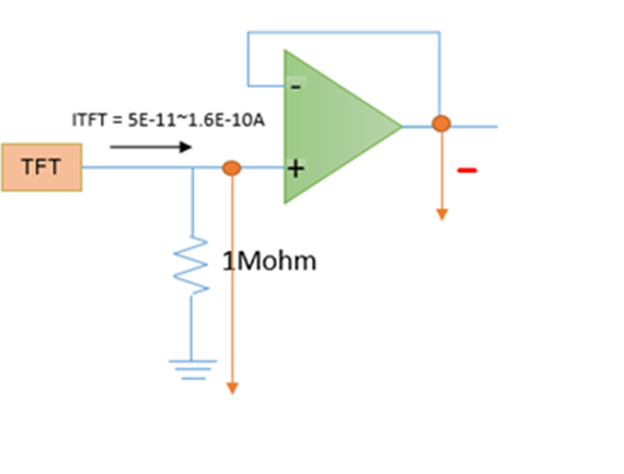
    My customer would like to do below config. For the output voltage vs temp, I see the voltage waveform is changing a lot when low temp. I am wondering if the root cause is the IB or not.

    Regards,

    Roy

  • Hello Roy,

    Thanks for the clarification. How much is a lot? Could condensation creating leakage current be the problem? 

    50pA to 150pA input is small versus typical IIB of +/-70pA. The output voltage of 50uV to 160uV is also very small. Is the op amp powered by dual supplies? The output is far too small for single supply.   

    Is this a new design?

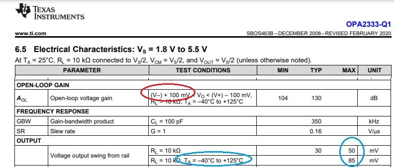
  • I think the issue is that you probably power the OPA2333-Q1 from a single supply.  Even though the input common-mode voltage includes the negative rail (GND), op amp output CANNOT get all the way to its rail but by connecting 1M resistor to ground you drive the output to ground.  In the case of OPA2333-Q1 the LINEAR (AOL condition) output voltage range is specified at 100mV from either rail while the NON-linear output swing is from typical 30mV to 85mV depending on temperature (see below).  Thus, I believe what you see is the non-linear output variation with temperature (Ron of output transistor vs temp) where output is completed trioded - slammed against its negative rail (GND) .