This thread has been locked.

If you have a related question, please click the "Ask a related question" button in the top right corner. The newly created question will be automatically linked to this question.

PGA855: Can PGA855 drive ADC with sampling rate > 1 MSPS?

Part Number: PGA855
Other Parts Discussed in Thread: ADS8900B, THS4551, THS4541, THS7001, , LMH6629, PGA870

Tool/software:

We would like to use the PGA855 to directly drive an AD9653 16-bit ADC running at 20 MSPS. The maximum frequency of the signals is 1 MHz sine wave. 

The PGA855 makes the statement that it can only directly drive ADC with sample rates up to 1 MSPS. I need help understanding the limitation.

Why does the PGA care about the ADC sample rate? What is the reason for that limitation?

And the PGA855 datasheet claims to have a bandwidth of 10 MHz.Even at 1 MHz bandwidth, a 1 MSPS ADC is pretty low and would only be good for a couple hundred KHz. What is the point of having a PGA with 10 MHz bandwidth if you can only use it up to say 200 KHz?

  • I should mention, I thought it might have to do with the analog input capacitance of the ADC. But the ADS8900B mentioned in the datasheet has 60 pF on the analog inputs, while the AD9653 only has 7 pF. It seems like it would take alot more current to charge the ADS8900B.

  • Hi David,

    The PGA855 is a precision programmable gain amplifier with ~10-MHz of BW. The PGA855 performance and ADC drive capability behaves in the expected and similar fashion, as most precision operational amplifiers, instrumentation amplifiers, and fully-differential amplifiers that offer a BW at around the ~10-MHz range. The PGA855 ADC output drive, small-signal, and large signal frequency response, and THD performance is consistent with other amplifiers offering a ~10 to ~20 MHz BW. 

    There are different ADC topologies, presenting different amplifier ADC drive requirements: mid-precision and high-precision SAR ADCs, precision/high-resolution Delta-Sigma ADCs, and high-speed pipeline ADCs. Many ADCs are un-buffered, where the external amplifier must drive directly the sample-and-hold capacitor, while other ADCs feature internal buffer amplifiers, or pre-charge buffers, making them easy to drive, and allowing the amplifier to support higher sampling rates. Therefore, the ADC amplifier drive requirements vary depending on the ADC architecture, the ADC’s sample-and-hold capacitor/structure, whether the ADC offers integrated buffers or pre-charge buffers, the ADC bit resolution, and the ADC sampling rate.

    The PGA855 data sheet recommendation of 1-MSPS sampling rate is conservative, and refers primarily to high-resolution (16-,18-, 20-bit), precision un-buffered SARs. On a SAR ADC During the acquisition phase, the driver amplifier must charge the converter’s internal sample and hold capacitor.  The voltage on the sample-and-hold must settle within ½-Least significant bit (LSB) of the resolution of the ADC.  Hence, the higher the ADC resolution, the smaller the LSB, requiring the external circuit to settle to a much smaller error window. On most SARs, the acquisition time is inversely proportional to the sampling rate, and therefore, the acquisition time can be very short at fast sampling rates.

    For example, the ADS9234 is an un-buffered 16-bit SAR ADC supporting a sampling rate of 3.5-MSPS, the acquisition phase can be as short 140ns at 3.5-MSPS. A high-speed fully-differential such as the THS4551 (150-MHz) is in most cases recommended/required to be able to drive and settle in the very short acquisition time, within the required 16-Bit SAR resolution, while offering optimal THD performance. 

    Hence, depending on the acquisition time, the ADC resolution, and sample-and-hold capacitor, the PGA855 may be able to support around 1-MSPS  to 2-MSPS sampling rates on un-buffered SAR ADCs. Keep in mind, this trend of ADC drive performance vs amplifier BW is also true for other standard op-amps or instrumentation amplifiers at the 10-MHz to 20-MHz BW and it is not a limitation specific to the PGA855.  

    The ADC you mention on the post above, is a high-speed pipeline ADC, supporting up to 120-MSPS, that you want to operate at 20-MSPS. I don't have detailed information on this ADC since this is from a different manufacturer.  However please consider the following:

    • The “Analog Input Considerations” of this pipe-line ADC data sheet states the signal source must be capable of charging the sample capacitors and settling within one-half of a clock cycle, when the input circuit is switched to sample mode.
    • Most applications requiring low distortion or high THD performance while supporting a 2-MHz input signal will unavoidably require a much faster amplifier than ~10-MHz. As you have mentioned, the PGA855 is a precision Programmable Gain Amplifier with a GBW of 10-MHz. As any other amplifier with a bandwidth around 10-MHz range, the THD performance is specified for signal up to ~40-50 KHz as shown on the figures 7-54, 7-55, 7-56 on page 18 of the PGA855 data sheet; where the THD starts to slowly degrade at input frequencies much above ~50kHz. 
    • For example, to provide perspective on the amplifier THD vs BW trade-off, below are data sheet THD performance plots of a couple of much higher bandwidth fully differential amplifiers (BW >100-MHz). At a input frequency of 2-MHz, the THS4551 (150-MHz) offers HD3 distortion at -80dB. If the circuit Designer has a strict THD performance at the -110dB level for a 2-MHz input signal, they will require the THS4541 that offers a BW of 500MHz.

    The PGA855 will support the 2-MHz input signal at 2V amplitude as shown on the plot below, but the amplifier will be close to its slew rate limit causing distortion... However, if your application requires very low distortion performance at fin= 2-MHz, or requires a higher output amplitude signal, the application will need a faster amplifier than 10-MHz.  See figure 7-41, large-signal step response vs frequency from the PGA855 data sheet:

    In most cases, circuit designers generally pair high-speed pipeline ADCs with high-speed, high-bandwidth FDAs with bandwidths well above the 100-MHz range for all these reasons.

    Thank you and Regards,

    Luis

  • Hello Luis,

    I really appreciate the detailed answer. Looks like we have been some things to think about. The most concerning is the THD charts that stop at 40 KHz :-). I'm guessing it is not good at 1 MHz.

    I had taken a simple minded view that the AD9653 has a 7 pF input cap. At 20 MHz, half a clock cycle is 25 ns. So using

    C = Q/V = i * dt /V

    we would need a current of i = C * V / dt = 7e-12 * 1 / 25e-9 = 0.3 mA even for a full 1 V charge.

    By comparison, the ADS8900B mentioned in the PGA855 datasheet has dt=500 ns (at 1 MSPS), V = 5V and C = 60 pF giving 0.6 mA. Seemed like we were ok.

    I notice PGA855 Figure 7-48 for the output voltage vs output current only goes down to 13V. We were going to set LVDD to around 2.0V. So it's not even clear how much current the PGA855 can drive.

    We've used the THS7001 for many years, but it is huge and has single ended output. We were hoping to simplify things. 

    Regards,

    Dave Hand

  • Hi David,

    Thank you for your additional details on the ADC drive requirements.

    In the ADS8900B 20-B SAR and precision SARs, the max sampling rate is typically related to the settling due to the time constants involved. In many cases, the settling time will be limited by the effective amplifier output impedance over frequency. To optimize the amplifier + filter + ADC circuit, simplified ADC models are used, where the transient response/settling/stability behavior is simulated, and then we verify/optimize the solution using bench measurements. On the ADS89xxB, during each conversion cycle, the 60pF S/H capacitor, charge loss after every conversion cycle is about 5% to 10% of the charge, where the sample-and-hold does not reset to 0V. The "average" ADS89xx input current is small, approximately at the ~ 20µA range, when supporting an acquisition time of about 300ns at 1-MSPS; hence the limitation is not due to the average input current. When driving the sample-and-hold, a percentage of the instantaneous charge during acquisition comes from the external R-C-R filter, where the external filter capacitor is is set  larger than the sample-and-hold, and the remainder of the charge is supplied by the amplifier driver. The amplifier output only sees around roughly a ~20mV step drop after each conversion for a 5V differential voltage.

    Nevertheless, you have a good point that the sampling and hold is much smaller, and the settling requirements and THD requirements are much more stringent for the 20-B SAR, with SNR at 101dB and THD -120dB level, compared to SINAD of 78dBFS for the pipeline so these target specs are different.

    The THD of the THS7001 (70-MHz) is -69dBc at 1-MHz typical. The PGA855 (10-MHz) does not spec THD at ~1-MHz, but extrapolating the data sheet curves, I would expect roughly at the -55dB to -60dB level. Let me know if this is acceptable.

    The minimum PGA855 output supply for LVDD and LVSS is 4.5V; so we would need to use Schottky input protection clamps between the ADC and PGA855, if the ADC is powered with a ~1.8V or ~1.9V supply. 

    I will spend time simulating the setting with 7pF sample-and-hold with the 25nS acquisition, assuming the 7pF S/H resets all charge, since I don't have the ADC behavior detailed model; but at a quick glance, I was not able to get close to the 16-bit level settling at the fast acquisition time. I will assume the max differential voltage is 2V.  

    Thank you and Regards,

    Luis


  • Hello Luis,

    We could live with 60dB. I also attempted to extrapolate the THD curves (printed it out and used a ruler), but that assumes it is linear (eg the THS7001 is not). Going from 40 KHz to 1 MHz is quite a jump.

    Also, the curves have assumptions that will not be valid in our case. For example, Fig 7-54 assumes a 10 Hz to 22kHz band-pass filter. Fig 7-55 has 10 Hz to 500 KHz (that's the one I used).

    We have the PGA855 eval board and will try to actually measure what it is doing at higher frequencies.

    We also have a Frankenstein monster of eval boards (AD9653 val + FPGA val + processor eval) that can read the ADC. We may try to drive the AD9653 with the PGA855 and see what happens.

    I agree the AD9653 is not clear on some points such as if it discharges the sample and hold cap. So it is not clear if it has to swing the entire 2V range. However, 20 MSPS is actually not all that high for 1 MHz wave. A 20'th of a wave is 18 degrees, so it might have to swing A*sin(18) = 0.3V even if the cap does not discharge.

    The maximum analog input voltage of the AD9653 is 2.0V, so we knew we would need extra clamps. It's a shame it does not have better protection.

    We attempted to simulate the PAG855 using these frequencies and it seemed fine. But we were using LTSpice and it is not always clear what simulation models include. 

    Thanks again,
    Dave

  • Thank you Dave,

    Let me discuss with the pipeline ADC experts. I suspect the SAR topology is more demanding from the settling perspective, since on the SAR, the settling error produce non-linear errors due to the binary weighted conversion process. However, this is not necessarily the case for other ADC types, that reset the sample-and-hold and have a smaller S/H capacitor, where the S/H resets to 0V or a fixed DC voltage.  On those, the settling error 'may' only translate to a small gain error. I would need to ask about the pipeline ADC behavior. Also, I will see if I can find data or bench performance about the THD at 1-MHz.

    Many Thanks,

    Luis

  • Hello Luis,

    I misspoke when I said the used LTSpice. They used TI Tina and PSpice. We never got the encrypted spice model to import into LTSpice.

    We did a quick check using the PGA855 eval board and the results did not look encouraging. We drive one side with an 80 mV 1 MHz signal and left the other side grounded. We had a harmonic at 3 MHz that was only about 35 dB below the main. We saw nothing at 2 MHz.  

    We need to check that we had proper coupling etc, but it does not look promising. Even if it can drive the ADC, with or without a buffer, that does not help us if the signal is distorted.

    One thing that seemed odd was even the gain seemed off. We ran with the PGA855 at maximum gain (ie 16) and it appeared to be down by about 30%. According to the plot on the first page of the datasheet (ie "Gain vs Frequency"), at least the gain at 1 MHz should be fine. But then one of the guys said that that is what they saw in the simulation as well. Is is possible the PGA855 spice model differs from the datasheet?

    But if the signal is highly distorted at 1 MHz and above, I have to wonder how they made the measurements for the "Gain vs Frequency" plot? What does it mean to say:

    ... offers excellent gain flatness, even at high frequencies ...

    if the signal itself is highly distorted?

     If you can find more info about the THD and other issues, maybe there is a way to make it work. But at the moment we are assuming we have to look for another solution. A fully differential version of the THS7001 in a much smaller package would be great :-). Don't suppose you have that in the works. We are a bit concerned about using a 27 year old chip in a new design and find it hard to believe it is still the best solution.

    In any event, we really appreciate all your help.

    Thanks,
    Dave

  • Hi David,

    The device is likely outside its valid linear range.

    The input common-mode voltage requires more than 2.5V headroom away from the input stage supplies VS+/VS-. The VOCM pin also requires at least 1.5V headroom away from the LVDD+/LVSS- output stage supplies.  In short, the device needs to be operated with ±bipolar input and output supplies in this case.

    • If the PGA (IN-) input is grounded, you will need the negative input supply VS- < -2.5V or more negative depending on the signal amplitude and PGA gain settings. I suggest using input stage supplies of VS+ = +5V, VS- = -5V for your initial test debug.
    • The VOCM requires a 1.5V headroom away from the output stage power supplies. Since the output common-mode is required at VOCM= 0.9V while supporting a 2Vpp fully-differential signal for the pipeline ADC, your negative output stage negative supply needs to be more negative than LVSS- < -0.6V. I suggest using LVDD+ = +5V and LVSS- = < -5V, VOCM = 0.9 for the initial debug.
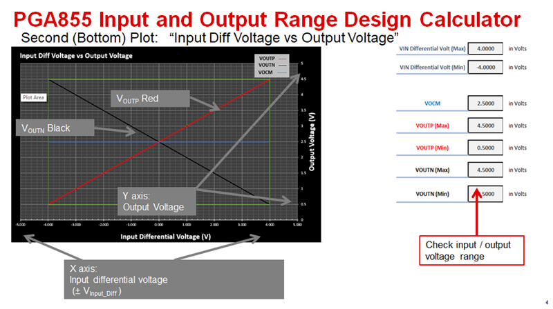
    • We offer a PGA855 input and output range calculator to verify the device is operated in range for different input voltage conditions, supplies and PGA settings.  At the bottom of this post is a snapshot/explanation of the PGA855 Input and Output Voltage Range Design Calculator tool.
    • Yes, The PGA855 and amplifier devices go through a thorough validation and devices are tested for performance. The frequency response of figure 7-40 shows the expected bench measured performance. However, the device needs to be operated inside its valid linear range. If you want to reproduce the full bandwidth data sheet plot on your bench using the eval board, you will need to remove all the default input and output R-C-R low-pass filters on the PGA855EVM, and use the data sheet test conditions: use a 50pF differential output capacitor load and 10k resistor load.  Keep in mind, this is the small-signal frequency response when driving the device in fully-differential fashion, with the device operating within is linear region.
    • Discussed with the high-speed ADC group. When connecting the ADC, the ADC input will require an optimal R-C-R input filter as shown below for the pipeline ADC drive. Use very low capacitance, low forward voltage Schottky diodes for protection. Schottky diodes with 1pF capacitance are available on the web.

    • You will need to place this ADC filter in very close proximity to the ADC inputs, with minimal parasitic capacitance/inductance on the connections between the ADC and the amplifier. Ideally one would use a dedicated PCB board were the PGA855 and ADC in the same PCB board.  If you are using separate PCB boards, you will need to use very short connections, and it may be a challenge to get optimal performance.

    • As we discussed, we do not specify THD performance at 2-MHz for the PGA855, but will perform a test in the next few days and update. The device does offer the flat small-signal gain response to 10-MHz, and the distortion performance is the consistent with that of a 10-MHz amplifier.

    • Let me know if you need a call.  Unfortunately, I am not aware of any replacement for the THS7001 (70-MHz) device. The PGA855 BW is limited to 10MHz which is considerably lower than the device you are attempting to replace, so in general, this device is not intended for a pipeline high-speed ADC converter. In most cases, circuit designers generally pair high-speed pipeline ADCs with high-speed, high-bandwidth FDAs with much higher bandwidths.

    Thank you, 

    Luis

    ---------------------------------

    Regarding the PGA855 Input and Output Range Design Calculator:

    The designer fills the cells in blue, that is, input supplies VS+, VS-; output supplies LVDD+, LVSS-; VOCM voltage, and PGA Gain.   You can change the input common-mode voltage using the VICM scroll bar. The input common-mode (VICM) is the average voltage of the inputs

    VICM = [(IN+)  + (IN-)] / 2

     The calculator provides a plot with the input-common mode voltage vs output voltage range. 

    The fields at the right side show you the max and minimum input and output voltage range for a given input common-mode as a function of the supplies, gain and VOCM voltage.

    The bottom plot on the calculator shows the “PGA855 Input Differential Vs Output Voltage”, and the tool provides the min/max OutP and OutN pin voltage ranges as a function of the supplies, VOCM voltage and PGA Gain inputs.

    You can download the PGA855 excel calculator tool in this link:

    https://www.ti.com/tool/download/PGA85X-INPUT-OUTPUT-RANGE-DESIGN-CALC

  • Luis,

    Support just does not get any better than the help you have given us!

    We were in fact powering the rails at +-15V. I think we can redesign our system to use much lower rails (after all, the ADC only takes 2 V). I will pass along all the info you have provided to our guys. We will take a few days to more methodically test things based on the info you provided. 

    Maybe there is hope yet for this chip.

    Thanks again,

    Dave

  • Hi David,

    Below is a quick measurement with the PGA855EVM.  The device is powered up with Vs+/Vs- = ±5V (input supplies); LVDD+/LVSS- = ±5V (output stage supplies, VOCM driven to +0.9V.  Removed the PGA855EVM filter input capacitors (C6, C13, C10), Removed the PGA855EVM filter output capacitors (C7, C8, C11).  The input signal is 2-MHz ±1Vp (2Vpp differential).

    The small signal response (100mVpp differential) looks good over all providing the expected small signal response, here is a 2MHz PGA855 osc plot with no input nor output filter; with G=1 (expected small-signal response was observed at other gains and the 16-B function generator has some noise, which is not filtered in this quick 2-MHz measurement)

    For the large signal response, the PGA855 out+ and out- oscilloscope plot is below, showing the expected 2-MHz ±500mVp (1Vpp differential) output signal at 2-MHz. However, I should mention, if I increased the signal closer to the 2Vpp differential at 2-MHz, I was already getting to the PGA855 large signal slew limitation, and could start to see the amplifier output waverform shows signs of distortion . This is not surprising, as this is shown on the PGA855 data sheet plot figure 7-41, at 2V differential signal, you are right at the limit.

    For a quick estimate of HD2 and HD3, I used a 1-MHz bandpass filter (passive LC filter) readily available in our lab, between the signal function generator and the PGA IN+ input. The PGA855 output was buffered with a high-speed, low noise, low distortion amplifier (LMH6629) and fed into an spectrum analyzer. 

    The PGA855 oscilloscope output measurement is below, showing the low noise the expected 1-MHz ±1Vp (2Vpp differential) output signal:

    The HD2 and HD3 at 1-MHz ±1Vp (2Vpp differential) output signal is below, HD2 is roughly around -65dB and HD3 is around -60.5dB.

    In summary:

             - The small-signal frequency response shown on the data sheet measures well on the EVM after removing the RC filters.  

    - Regarding the large signal, if you require a 2Vpp 1MHz signal, the device measures distortion at the -55dB to -60dB level, as we estimated before.

    - At 2-MHz, 1Vpp, the response is fine without any noticeable gross distortion. 

    - However, as you start to increase amplitude between 1.5Vpp to 2Vpp at fin = 2MHz, the PGA855 output signal shows signs of distortion.  This is expected, as you are getting to the slew-rate limitation of the device, and the response is not optimal there.

    Hope this helps,

    Thank you and Kind Regards,

    Luis 

  • Luis,

    It will take us a little while to process all the info and also to make sure the PGA855 can drive the AD9653.We have a setup to do that.

    We're also looking at other options such as the PGA870.

    Thanks again,
    Dave

  • I double checked and we had not in fact removed the input and output low-pass filters as you suggest above. Based on, for example TI's:

    Three guidelines for designing anti-aliasing filters

    given R = 100 ohm and C = 100 pF we get Fc = 8 MHz for the 3dB point. So at 1 MHz, it would be essentially passed through. At 2 MHz, it seems there would be at least a 3% drop, so removing them would make sense in that case.

    Of course, given component tolerances for caps it probably makes sense to just remove them. And our tests were at 15V. I suspect that was why we were seeing so much distortion. The waves looked ok visually, but the harmonic distortion was pretty low.

    If we can't make the PGA870 work, we'll redo our tests as you suggest.

  • Hi David,

    Yes, the THS7001 (100-MHz (-3dB), Slew Rate=175 V/µs) high-speed PGA we are trying to replace is an order of magnitude faster than the PGA855.  

    The PGA855 (10-MHz, Slew Rate = 35V/µs) is not considered a high-speed amplifier; this is a high precision instrumentation amplifier for much lower bandwidth applications. The limit in distortion performance at the high frequencies is not only due to the small-signal bandwidth limitation, but also due to the slew rate limit of 35V/µs. See figure 7-41 "Large-Signal Step Response vs Frequency".  The 2Vpp, 2MHz signal amplitude is close to the Large Signal Step Response boundary, and sinusoidal signals getting close to the boundary will show distortion degradation as the input signal amplitude/frequency starts to reach the slew-rate limit. 

    As we discussed, I measured HD3 at 2Vpp 1MHz at around -55dB to -60dB; but also measured significant distortion degradation at 2Vpp 2MHz.  This is due to the slew rate limit (in addition to the 10-MHz BW limit), whether you use ±15V supplies or ±5V supplies.

    The PGA855 (10-MHz, Slew Rate = 35V/µs) is primarily intended for DC precision/high resolution SARs and Delta-Sigma ADCs, supporting good AC performance with AC signals at the many 10s KHz to ~100kHz range.  The device should be compared with other high precision instrumentation amplifiers in its class. 

    You are correct, high-speed PGAs such as the THS7001 (100-MHz (-3dB), Slew Rate=175 V/µs ) and PGA870 (600-MHz, Slew rate=2900 V/µs ) offer significant higher BW, and slew-rate, and specify distortion at much higher frequencies; producing the very low distortion result at 2-MHz.  These are optimal devices to drive the high-speed pipeline ADCs.  

    Thank you,

    Luis