Part Number: PGA855
Tool/software:
Hi Caro,
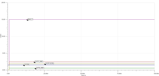
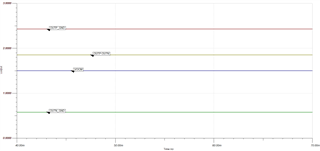
I have simulated this part using the macromodel, you can see the setup in the image below.
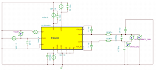
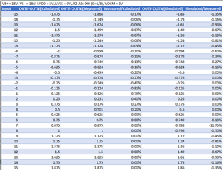
VS+ = +18V, VS- = -18V, LVDD = 3.3V, LVSS = GND, A0=A1=A2=GND (Gain of 0.125), INN = GND, VOCM = 1.5V, INP = Step input applied.
I am using an attenuating gain of 1/8.
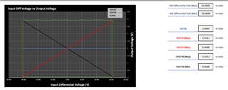
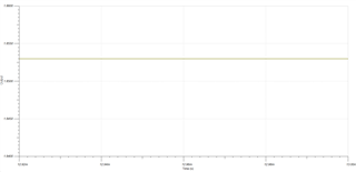
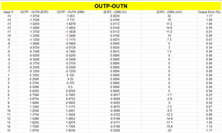
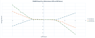
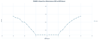
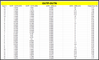
For the INP Pin I applied a step input of -15V up to +15V in 1V steps (in separate simulations) and measured the output differential Voltage (OUTP-OUTN).
I compiled the following table of results of the expected output VS the simulated results and got the delta of those data points, see the table below with the associated error (in %).
See the plot below of the delta between expected and simulated results across the step input range.
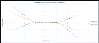
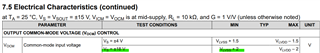
Based on the datahseet of this part I am not sure to understand where this magnitude of error is coming from, perhaps I am missing something, would you be able to explain the results I am seeing?
I have configured this part up similarly (in another simulation) to that of the PGAEVM schematic and see similar results to those above for this gain.
Thanks in advance for your response.