This thread has been locked.

If you have a related question, please click the "Ask a related question" button in the top right corner. The newly created question will be automatically linked to this question.

OPA4H014-SEP: Bootstrapping the negative supply of OPA4H014-SEP to mitigate input capacitance concerns

Part Number: OPA4H014-SEP

Tool/software:

Hello,

I am trying to use an front-end amplifier on a small capacitive sensor (0.033-0.1pF) for a space application. I like the OPA4H014-SEP because of its low bias current, current and voltage noise densities, and relatively low common mode input capacitance. In order to increase the sensitivity of the measurement in relation to the sensor, I want to employ a bootstrapped connection to the negative terminal of the op amp as shown below (using Rb, Cb, the unnamed op amp gate, Cv and Rp):
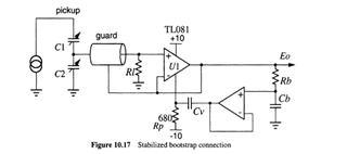
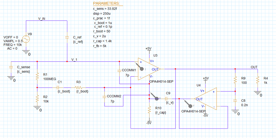
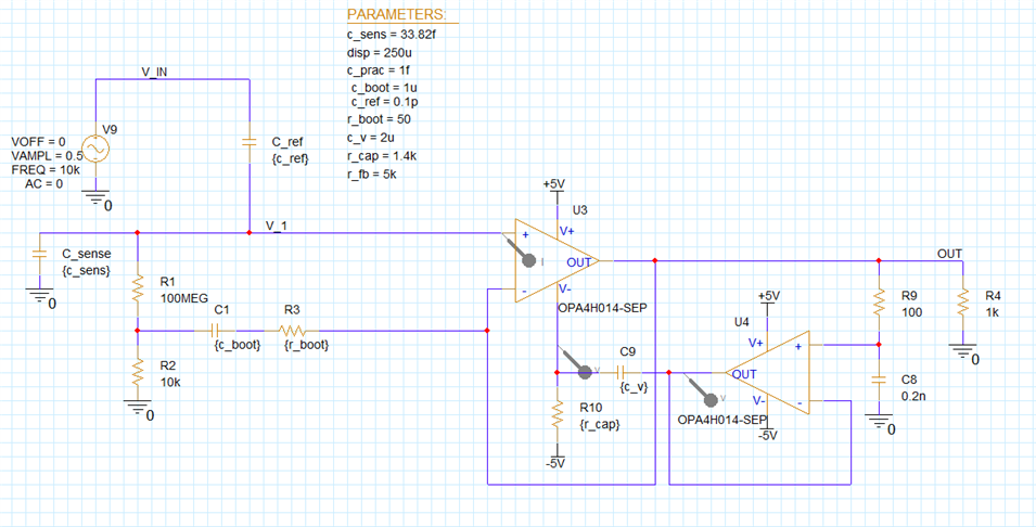
Based on what I was reading, this should effectively decrease the effects of the common mode input capacitance IF the common mode input capacitance is connected to the negative supply. I was looking at the PSPICE model for this part but was struggling to identify if this is the case for this part. When I run simulations with this topology, I do not get the intented effect. If I comment out the common mode capacitances on both inputs and add discrete capacitors of the same value to my simulation (with one end of the capacitor being on the input and the other being on the negative supply pin), I do get the intended effect. A picture of my current simulation set-up is shown below:
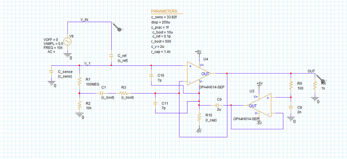
I want to know if this is a valid change to make for the sake of simulations, or if you have any alternate recommendations for bootstrapping out the effects of the common-mode capacitance. Alternately, if you know of a part with similar noise densities and input bias current but with a smaller common mode capacitance, that would be great. The input signal is 10kHz so the bandwidth just needs to be enough to support this. Thanks!

  • Hi Cameron,

    I am not sure the purposes of the circuit. 

    Here is something that you need to keep in mind. 

    1. The quiescent current needs to be meet up to 3mA + load current. 

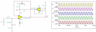
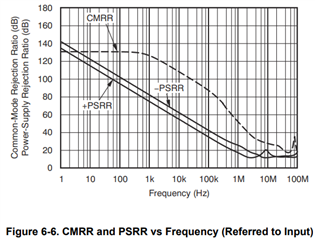
    2. When OPA4H014-SEP is fed back to Vee rail, there is PSRR attenuation at 10kHz. At Vee rail, -PSRR attenuated the negative supply rail at 60dB range @10kHz. So the fed back signal at Vp1 is attenuated at 60dB at the Vout. At Vp1 node, the output amplifier 10kHz is riding on the (Vee - 1.4kΩ*Iee), see the simulation. 


    I think that you include some of parasitic capacitance and I removed these in the above simulation.

    OPA4H014-SEP E2E 11202024.TSC 

    3. I simplified the input, where the input capacitance is C1 + C2 and adjusted the Thevenin's voltage from your 0.5V @10kHz at your VIN input. 

    Please let me know if you have additional questions. 

    Best,

    Raymond

  • Hey Raymond,

    The purpose of the entire circuit is to measure the capacitance of the capacitor labeled C_sense in my simulation. This value will be from 0.02-0.1pF. Currently I am setting it at a nominal case of 33.8 fF.

    The purpose of the U3, C9, and R10 (as referenced on the screenshot from my simulation) is to attempt to mitigate the effects of this input capacitance on my measurement.

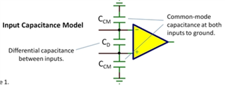
    The parasitic capacitors in my simulation are attempting to model the common-mode input capacitance shown on the data sheet:


    I note that the common mode capacitance is already in the PSPICE model for this part:

    However, I was not able to get the simulation working with this model so I commented out the two lines in the PSPICE model and tried it with the discrete capacitors tied directly to the negative supply. I am unsure if this is a fair assumption to make, or if the common-mode capacitors of the op amp are truly unaffected by the bootstrapping technique I am employing.

    Here is the simulations when I try commenting out the common-mode capacitances in the PSPICE model and placing discrete capacitors to mimic them in the simulation.

    Here are these two lines commented out.

    Here is the simulation that I am running with CCOMM1 and CCOMM2 being used to mimic the common mode capacitances.

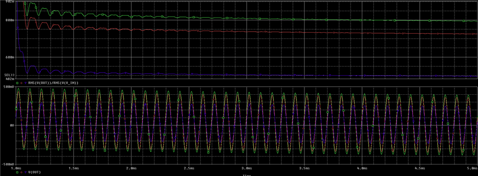
    I am varying the capacitance C_sense with the following values: 0.02pF, 0.033pF, 0.1pF.

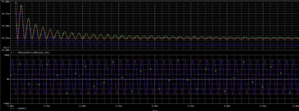
    Here are the results:

    The RMS value of the output to the input is really what I am most concerned about as I am trying to maximize the sensitivity of the circuit to changes in C_sense. This roughly lines up with the math on the capacitive divider if the parasitic capacitance is 0, which is the desired result:

    G = V_out / V_in = C_ref / [C_ref + C_sense + C_parasitics]

    G (C_sense = 0.02p) = 0.833

    G (C_sense = 0.033p) = 0.747

    G (C_sense = 0.1p) = 0.5

    If I delete CCOMM1 and CCOMM2 and revert the PSPICE model back to its original state, I get these results:

    These results do roughly line up with a parasitic capacitance of 7pF:

    G = V_out / V_in = C_ref / [C_ref + C_sense + C_parasitics]

    G (C_sense = 0.02p) = 0.014

    G (C_sense = 0.033p) = 0.014

    G (C_sense = 0.1p) = 0.0139

    I tried using the discrete capacitors because some of the references I looked into said to treat the common-mode capacitance as connected to the negative supply (e.g. https://e2e.ti.com/blogs_/archives/b/thesignal/posts/input-capacitance-common-mode-differential-huh). Is this assumption not valid for OPA4H014-SEP or am I missing something? As I understand it, PSRR would not affect how the input capacitance is mitigated, but maybe I am misunderstanding something there.

    Is there an alternative way to mitigate this input capacitance or a better op amp with a similar bias current and noise densities?

  • Hi Cameron,

    Is there an alternative way to mitigate this input capacitance or a better op amp with a similar bias current and noise densities?

    Yes, the typical differential and common input capacitance are already incorporated in the Spice model. So it is not needed to include these. 

    This value will be from 0.02-0.1pF. Currently I am setting it at a nominal case of 33.8 fF.

    This is going to be touch, since the parasitic capacitance of your PCB or leads have higher capacitance than the measured value. 

    The equation of the technique is based on CdV/dt = I, where I is the constant current source.  

    1. if V=Asin(ωt), where A is the 10kHz or higher frequency's amplitude, dV/dt = Aω*cos(ωt) = Apk*2πf = Ipk/C

    The measured C = Ipk/Apk*2πf 

    2. The other method is using constant current I and driving the measured C directly, and measure dV/dt rise from 10kHz or higher frequency square wave. You have to use mosfet to charge and discharge capacitor from the constant current source. 

    In any case, the measured signal has to be high enough in order minimize the sensing errors.  You have to null out the circuit first and remove other parasitic capacitance from the sensing circuit.  

    Do you have to use space grade op amp to measure the C? Our space grade op amp with high precision specification is limited. Please let me know.

    Best,

    Raymond

  • Hey Raymond,

    I am guarding the traces for the sensing net, along with guarding the connector/cabling to the sensing capacitor, to mitigate parasitic capacitance concerns. The guard ring will be driven with the output voltage of the OPA4H014 to null the effects of these parasitic capacitances. Additionally, I will be utilizing a bandpass filter downstream to mitigate noise concerns.  

    What non-space options are available that have a lower input capacitance? I might be able to use them if need be.

    I am still confused about the input capacitance for the OPA4H014-SEP. Based on the reference I attached in the earlier comment (https://e2e.ti.com/blogs_/archives/b/thesignal/posts/input-capacitance-common-mode-differential-huh), it would seem that the common mode input capacitance should be tied to the negative supply rail, but this seems to not be the case for this part. What is the reason? Is there some intermediate stage or transistor topology on the IC that prevents this from being the case?

  • Hi Cameron,

    it would seem that the common mode input capacitance should be tied to the negative supply rail, but this seems to not be the case for this part. What is the reason?

    Cd is referenced between  Vcc and Vee (power rails' mid point). 

    Ccm+ is referenced between Vcc and the common reference or GND

    Ccm-, is referenced between Vee and the common reference or GND. 

    I am guarding the traces for the sensing net, along with guarding the connector/cabling to the sensing capacitor, to mitigate parasitic capacitance concerns.

    The drive guarding rings or traces are sensing input are to establish the same potential at the input node, which are to mitigates the effects by ensuring that no significant current flows through the capacitance. I do not believe that it will reduce the parasitic capacitance. 

    In your op amp circuit by sensing the parasitic input capacitance, the capacitance seems be to sub pF range. I am not sure that the circuit has the sensitivity to sense the <pF capacitor value in the configuration. The typical handheld or regular bench type LCR meter has tough time to measure sub pF capacitor value. 

    You would need to increase the signal generator's frequency up to 1MHz in order to sense the parasitic capacitance (Xc = 1/sC). 10kHz may be too low to measure it accurately. What is the measurement accuracy per your application?

    Best,

    Raymond