This thread has been locked.

If you have a related question, please click the "Ask a related question" button in the top right corner. The newly created question will be automatically linked to this question.

INA350: Can I reduce offset by software?

Part Number: INA350
Other Parts Discussed in Thread: INA351

Tool/software:
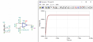
When REF connect to GND, this circuit output 8.86mV.

When REF connect to 1.65V, this circuit output 1.65V.

Why does different REF get different offset?

When REF=1.65V, almost no offset.

When REF=0V, offset=8.86mV.

  • Hey Allen,

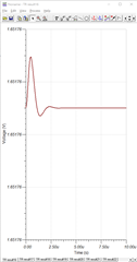
    There is a small offset on the output when the output is 1.65V, however, there are not enough digits being displayed on the Y axis to show the offset voltage.This offset is different than the "offset" seen when the Ref is 0V.

    Ideally, the output of the INA350 in the 1st condition should be 0V, however, your negative rail is 0V as well, so you will run into an output swing limitation.

    The output of the INA350 (and almost every amplifier device) will not swing perfectly to V-, as there is some voltage differential that must be on the output transistor.

    On the graph, double-click the y axis, and change the value of precision to 5-6.

    Best,
    Jerry

  • Sorry, I forgot to click it. the output voltage is 1.65176V.
    The offset voltage is less than 8.86mV. Why?

  • I wanted to simplify the circuit, so I connected VREF to ground and the ADC measured the output voltage, get the offset voltage. Then I connect signal to R7 to get sensor voltage cross R9(this is a resistance sensor). If I can get the correct offset voltage, I can minus it by software. Is this possible?

    Simulation result:

    1. REF=0V, VIN=0V( IN+ and IN- connect to GND with 330kOhm): Vo=8.86mV -> offset=8.86mV

    2. REF=1.65V, VIN=0V( IN+ and IN- connect to GND with 330kOhm): Vo=1.65176V -> offset=1.76mV
    For simulation result, 2nd result is more close to INA350 spec. Why is the offset voltage of 1st result too big?

  • Hey Allen,

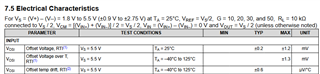
    The typical offset you should be seeing for the INA350 in a gain of 10 is ~2mV. In simulation you are seeing about 1.7mV of offset. This is the correct offset, not the 8mV when the output is not in a linear range.

    You can calibrate with software the initial offset of the amplifier. You will have to establish a minimum value, but you must make sure that the amplifier is in a linear operating range. The amplifier is not in a linear range when you are seeing the 8mV value. This 8mV value is not the offset, it is the amplifier reaching its output swing limitation. This can be checked in the analog engineers calculator (https://www.ti.com/tool/ANALOG-ENGINEER-CALC), or by reading the input and output swing ranges in the datasheet. Once the 0 value is established, your software can define the ADC value that is being read as your 0 value.

    This will calibrate out the DC offset, and the next source of error will be the offset drift of the amplifier. From the datasheet, it is 0.6uV/degC, referred to input. Therefore for a gain of 10, it will be 6uV/degC.

    Best,
    Jerry

  • Simulation result:

    1. REF=0V, VIN=0V( IN+ and IN- connect to GND with 330kOhm): Vo=8.86mV -> offset=8.86mV
    This is TINA simulation result.

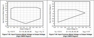
    Refer to the datasheet, input common-mode voltage should >0V.

    So if I want to get offset volatge, I should let IN+  and IN-  > 0.2V. Right?

    When REF=1.65V, input common-mode voltage should > 1.6V for high CMRR range. 

    But the 2nd simualtion result get the correct offset voltage. Why?


    I use INA351 for the same circuit. The simulation result is the same as INA350.

    When REF>0V,  IN+, IN- =0V, I can get close to spec offset voltage.

    When REF=0V, IN+, IN- =0V, I  can get bigger offset voltage than spec.

    Refer to upon picture, VG1 is MCU push-pull output. I can controll it forward and reverse that can generate a AC signal on R9.
    This circuit can measure the approximate impedance of R9. 

    And I want to controll VG=0V to get offset volage, then calibrate it by software. Is this possible?

    For simulation result by TINA, Let REF=0.3V or more can get the correct offset voltage.
    And when VG=3.3V, (Vo - offset volatge) can get the ideal voltage.

    The simulation result is correct?

  • Allen,

    When you are seeing error on the output when input and ref are 0V, that is not offset voltage. That is the output swing limitation of the output amplifier.

    The figures that you are referencing do not have enough resolution to show the limitation in output swing. For this we must reference the electrical characteristic table.

    No amplifier can output true 0V when V- is 0V.

    Even though it looks like the output can swing to 0 in the charts from the datasheet, the output can only swing to 15mV. The width of that line in the chart covers the difference between 0V and 15mV.

    Once the output is in a valid linear region, then any difference between input and output voltage is going to be the output-referred offset voltage. The datasheet specification provides the input-referred offset voltage. To translate the input-referred offset voltage to output-referred offset voltage, it will be the input-referred value times the gain of the amplifier.

    If VG = 0V, and Ref is 0.3V, then this will display the proper offset on the output of the amplifier, and this can be calibrated out. Trying to calibrate with input at 0V and ref at 0V, you will be setting the calibration point at output swing limitation, and the error will be worse than if you did no calibration at all.

    Best,
    Jerry

  • Trying to calibrate with input at 0V and ref at 0V
    -> I confused. You said:  OPA can't output real 0V. Output voltage will >15mV. But this output voltage is not real offset. How to get the offset voltage and calibrate it?

  • Hello Allen,

    Offset voltage will be the difference between Ref and output. Since your measurement will be single-ended, you can apply 0.3V ref to the INA350, read this value on the ADC, and then set that value as your 0 point. Now when a signal is applied, you will be measuring the difference between Ref and the signal.

    Best,
    Jerry

  • H Jerry

    Thanks. So INA350 need a REF like reference design if I want to cancel offset by software. But it will need a extra OPA as ref buffer.

    I will choose INA351 for this design.

  • Hey Allen,

    The requirement for REF is that it must be a low-impedance source. Therefore, you cannot create ref from a voltage divider, however, if you have a voltage reference that can source and sink current, then you do not need to buffer ref with an extra op amp.

    Adding a buffered reference will not hurt the performance of the circuit, just know that you do not need it in every circuit with INA350.

    Best,
    Jerry