Because of the holidays, TI E2E™ design support forum responses will be delayed from Dec. 25 through Jan. 2. Thank you for your patience.

THS4532: About THS4532 cal offset

Part Number: THS4532
Other Parts Discussed in Thread: THS2630

Tool/software:

Hi team,

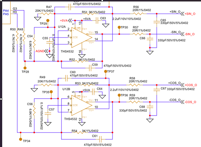
My customer's schematic is below. They want output offset as possible as equal to zero. Can some adjust method to improve? If change to THS2630, does the around component need to change? Thanks 

Input signal 2.31 Vp-p

Input offset 1.65V

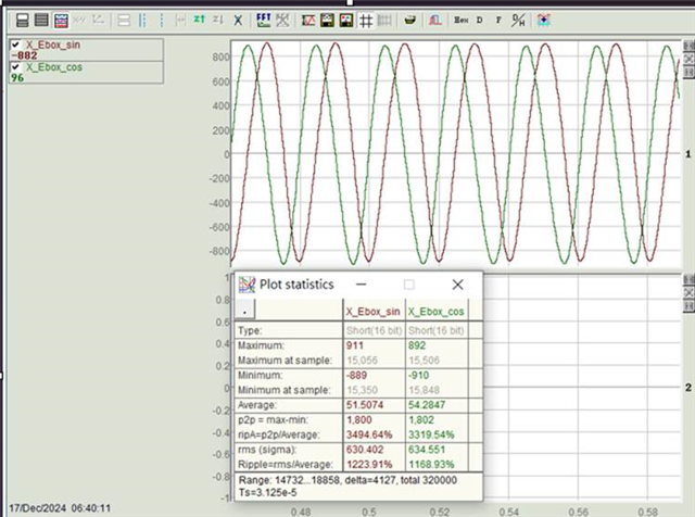
Pic2 is the output waveform as  SIN and COSIN

Sin is red and Max=911mV min=-889mV

Cosin is green and Max=892mV min=-910mV
  • Hi Jimmy, 

    In order to have accurate offset using fully differential amplifiers, you need to have the impedances balanced between the IN+ and IN- pins. In your current circuit you have a 4.7kOhm resistor on the signal input pin but a 20kOhm resistor to ground on the non-signal input. I would adjust the 20kOhm resistor to 4.7kOhms to properly balance the circuit. That should help remove offset. 

    Regards, 

    Jacob 

  • Hi Jacob,

    pls, see customer's reply. thanks 

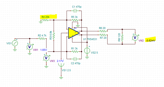
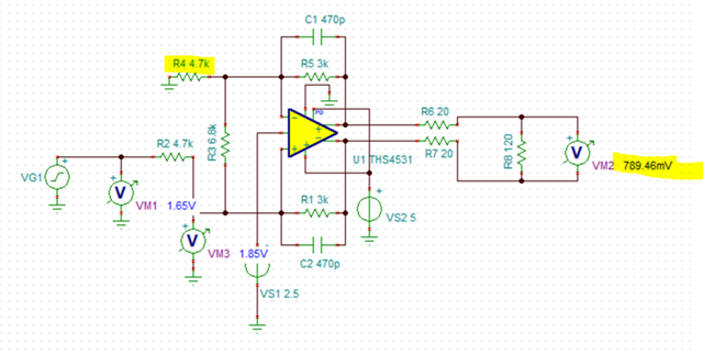
    I used the Ti simulation tool to simulate. In the simulation circuit (please refer to below) ,

    I changed the resistance of R4 (20k Ohm-->4.7k Ohm). As a result, the output DC bias was not optimized.

    Thank you .

  • HI Jimmy, 

    Thank you for the simulation I now see the additional issue. The signal input side of the circuit appears to have a DC value of 1.65V. That will cause an output offset because the non-signal side of the FDA input is simply terminated to ground. 

    There are two ways to deal with this. You can terminate the non-signal 4.7k Ohm resistor to 1.65V, or you can make a thevenin equivalent voltage divider on that input that has an impedance of 4.7k and creates an 1.65V bias. 

    Best, 

    Jacob