Part Number: OPA858-Q1
Other Parts Discussed in Thread: OPA858
Tool/software:
Subject: Query Regarding Unexpected Voltage Output in TIA Design
Dear [Recipient's Name],
I hope this message finds you well. I am encountering an issue with my transimpedance amplifier (TIA) design using the OPA858-Q1 op-amp, and I would greatly appreciate your insights.
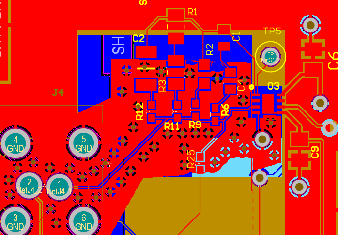
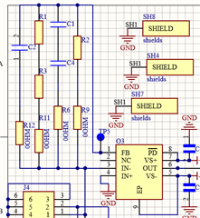
Details of my setup:
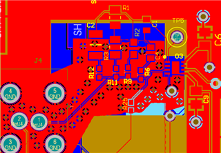
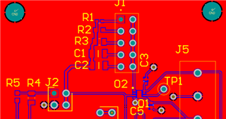
- PCB thickness: 4.2 mm
- Feedback resistor: 1 MΩ
- Non-inverting terminal connected to ground
- Inverting terminal connected to the signal
Observations:
- When the 1 MΩ feedback resistor is shorted and no input is applied to the inverting terminal, I measure an output voltage of 36 mV, whereas I expected it to reflect only the op-amp offset (0.8 mV as per the datasheet).
- When the 1 MΩ feedback resistor is connected (not shorted) and no input is applied to the inverting terminal, the output voltage is 12 mV.
Based on my understanding, the output voltages in both cases should ideally be close to the op-amp offset voltage. However, the measured values differ significantly.
Could you please help me identify potential sources of this discrepancy?
- Could it be due to PCB design factors such as parasitic capacitance or stray currents?
- Are there any other considerations in the layout or components that might explain this behavior?

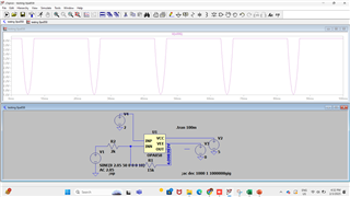
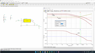
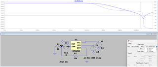
 without Cf
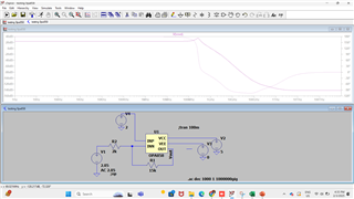
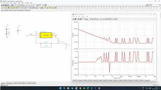
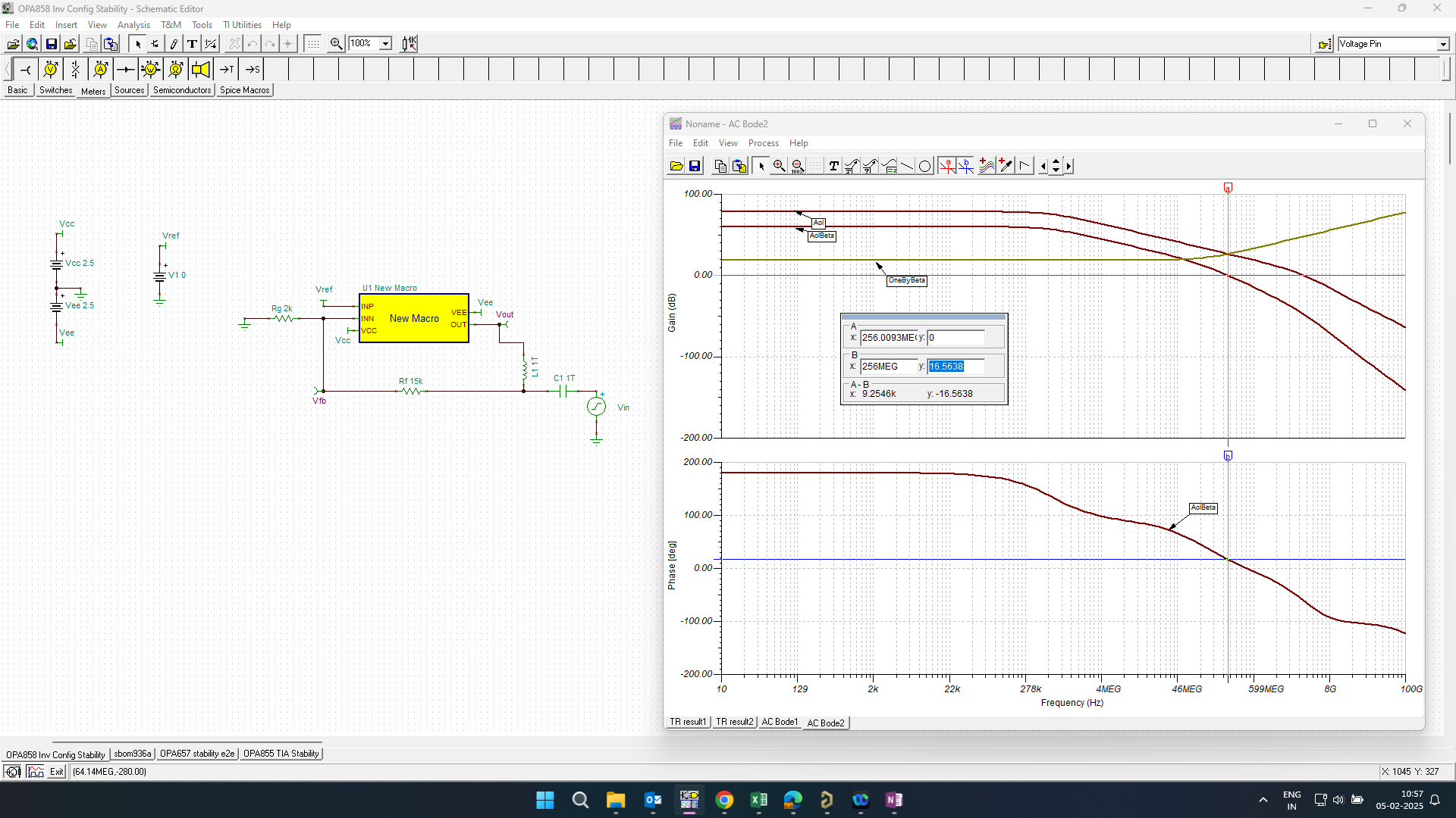
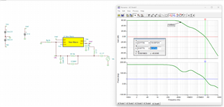 with Cf added
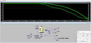
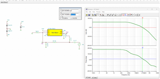
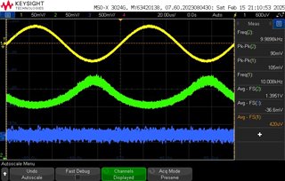 so yellow color graph is input which i gave from function generator , green color graph is the output of teh opamp where the sc is 1.36 .. and please ignore blue color graph , and the circuit layout diagram is attached