Other Parts Discussed in Thread: TLV3511
Tool/software:
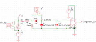
I am trying to design a circuit based on the LMV7219 comparator whose output is in sync with the positive half cycle of an AC voltage in the hundreds of kHz range. This is the circuit I currently have :

The voltage divider resistors are in the megaohm range because my circuit need to handle high input voltages at times. The capacitor C1 is added because my input could potentially have a DC component and I do not want that to impact the sensing of the AC component zero crossing.
However, when tested with my actual input signal or a function generator, there is a substantial phase shift between input AC signal and the comparator output. The output duty cycle is also far from 50% even when tested with pure AC.
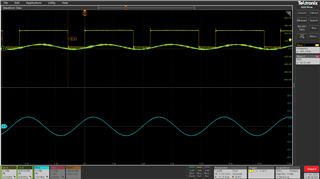
I noticed that when powered up w/o any input signal, there is a ~50 mV DC voltage on the non-inverting input pin of the LMV7219. When tested with a pure AC sine wave from a function generator, the waveform on the non-inverting input pin of the LMV7219 seems to have a dc offset.
Here are the test waveforms. The top two are the non inverting input and output of LMV7219. The bottom waveform is the test signal fed into the voltage divider from a function generator. In this test, the 10 Meg resistor is replaced with 1Meg.

I suspect the input offset/bias current of LMV7219 is causing my issues. Is there any tweaks I can make to compensate for this error? If there is no simple way to correct this, are there any drop-in replacement parts I can replace the LMV7219 with that does not have this offset/bias issue?
Thank you

