This thread has been locked.

If you have a related question, please click the "Ask a related question" button in the top right corner. The newly created question will be automatically linked to this question.

THS7530: THS7530

Part Number: THS7530
Other Parts Discussed in Thread: PGA855, INA159, INA500

Tool/software:

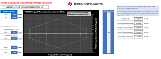
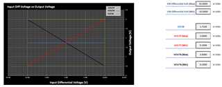
Hi, I need to design an analog front-end for differential signal acquisition. The ADC can be 1MSPS and powered with 3.3V or 5V, Vref=3V or 4.096V. The input ranges has to be +/-0.1V, +/-0.5V, +/-1V, +/-2V, +/-5V. We can use for example a programmable gain istrumentation amplifier driven by micro as first stage with input protection for overvoltage. Can you give us support for the chain design using your products? Can you suggest the best solution/architecture?   Thanks

  • Can you look at PGA855 to begin with.

    What is the distortion , rise time , 1% flat bandwidth required for this application ?

  • Hello, 

    The PGA855 is a good place to start, what supply voltages do you have available in your system? 

    Th PGA855 requires at least 8V in the front end. 

    All the best,
    Carolina

  • ADC we would like to use is a 16-bit connected to uC (STM32H743XI). At least 1MBPS. Vref=3V. Power supply of uC is 3.3V.We could use also the ADC integrated in the uC.

    Important is to have multi-range differential input of analog front-end, in particular +/-0.1V, +/-0.5V, +/-1V, +/-2V, +/-5V ranges programming the correct gains with PGIA (Programmable Gain Instrumentation Amplifier) in one or two stages before the ADC.

    For example…. +/-0.1V differential input…. 1st stage Amplification 100x ---> +/-10V ----> 2nd stage Attenuation 0.3x ---> +/-3V differential ADC range

    For example…. +/-0.5V differential input…. 1st stage Amplification 10x ---> +/-5V ----> 2nd stage Attenuation 0.6x ---> +/-3V differential ADC range

    For example…. +/-1V ............................

    ...................................

    something like that.

    We could program a PGIA (Programmable Gain Instrumentation Amplifier) by uC.

    First stage could be a protection stage (+/-5V is the maximum range)… zener diodes, TVS, fuses etc, eventually buffer to have saturation in the event of overvoltage. Second stage a PGIA but we have to be compliant to Vref of ADC for every range in the sense to change input amplification or attenuation (only for 5V) for optimization of the signal dynamics. I suppose that if power supply of ADC is 3.3V then Vref could be 3V or 2.5V so we need the corret gains, better if all is integrated but  if not possible we could use external precision resistors with analog switch to set amplification/attenuation.

    If PGIA is fully differential we could connect it to ADC… if necessary we could use a second fully differential stage and DPOTs.

    For ADC input protection we could use ultrafast diodes or buffer amplifier for saturation or voltage limiting amplifier before the ADC input.

    ADC Vref has to be a high precision reference.

    We have no info about the distortion , rise time , 1% flat bandwidth required for this application

    Can you support in the hw architecture to use? It is a new project for us, now we have to design a first prototype.

  • Power supply is 5V, 3.3V, but if necessary we could consider other power supplies.

  • Hello, 

    From your response, it's still unclear to me if you have dual supplies in your system - my assumption is that you would since there are voltages that are ±, but since you specified only single supply - my answer takes that into consideration (the output is limited 0 to 5V), this can be changed by moving VOCM to 0V (if dual supplies are present). 

    Here is my proposition, add a ±10V supply voltage to the system, this can be done by using the following device: TPS65131 data sheet, product information and support | TI.com

    Now that the system has dual supply at the input, the problem is solved using only the PGA855 -> ADC/MCU. The PGA855 has differential output stage and input overvoltage protection of up to 40V below or above the power supplies. 

    The ADC can be 1MSPS and powered with 3.3V or 5V, Vref=3V or 4.096V. The input ranges has to be +/-0.1V, +/-0.5V, +/-1V, +/-2V, +/-5V.

    I will walk through what gains to use for each input range, I used the Calculator Tool on the PGA855 product page: PGA85X-INPUT-OUTPUT-RANGE-DESIGN-CALC Calculation tool | TI.com

    All solutions use the following power supplies: VS+ = 10V, VS- = -10V, LVDD+ = 5V, LVSS- = 0V, VOCM = 1.75V (this can be made from resistor dividing Vref of the ADC or VS,LVSS), since the input ranges are centered around 0, I assumed VICM is 0V - if this isn't true please let me know. 

    Input Ranges Gain & VCM v VOUT Input Differential vs Output Voltage (Input*Gain+VOCM)
    ±0.1V

    G = 8 (110)

    For ±0.1V, the max input differential voltage is assumed to be -0.2V or 0.2V.

    At 0.2V diff, the ADC input would read 2.55V (0.1V*8+1.75).

    At -0.2V diff, the ADC input would read 0.95V (-0.1V*8+1.75).

    ±0.5V

    G = 2 (100)

    For ±0.5V, the max input differential voltage is assumed to be -1V or 1V.

    At 1V diff, the ADC input would read 2.75V (0.5V*2+1.75).

    At -1V diff, the ADC input would read 0.75V (-0.5V*2+1.75).

    ±1V

    G = 1 (011)

    For ±1V, max input differential voltage is assumed to be -2V or 2V.

    At 2V diff, the ADC input would read 2.75V (1V*1+1.75).

    At -2V diff, the ADC input would read 0.75V (-1V*1+1.75).

    ±2V

    G = 0.5 (010)

    For ±2V, max input differential voltage is assumed to be -4V or 4V.

    At 4V diff, the ADC input would read 2.75V (2V*0.5+1.75).

    At -4V diff, the ADC input would read 0.75V (-2V*0.5+1.75).

    ±5V

    G = 0.125 (000)

    For ±5V, max input differential voltage is assumed to be -10V or 10V.

    At 10V diff, the ADC input would read 2.375V (5V*0.125+1.75).

    At -10V diff, the ADC input would read 1.125V (-5V*0.125+1.75).

    G = 0.25 (001) *ALTERNATE SOLUTION*

    For ±5V, max input differential voltage is assumed to be -10V or 10V.

    At 10V diff, the ADC input would read 3V (5V*0.25+1.75).

    At -10V diff, the ADC input would read 0.5V (-5V*0.25+1.75).

    If you do not wish to add the dual supply, there is also the option of introducing a difference amplifier stage (INA500 - G =0.25, or INA159 - G = 0.2) in the front and then following up with a PGA, this will likely still not be enough input voltage common mode, and be a more inefficient design as this would add noise (diff amps) or less enob (INA500 inaccuracy).

    Please let me know which path forward you decide and if any of my assumptions are incorrect, I can help further. 

    All the best,
    Carolina 

  • Hi Carolina,

    thanks for your support... perfect your analysis.

    No problem for dual power supply, we can have it in our system. Most likely the input common mode will be zero or a few volts.

    We will have 16 bit on 3V range... could it be a problem that for ±5V diff input the ADC input would read 2.375V/1.125V, a slightly poorer dynamic than the other scales?

    As soon as possible I will give you more information about the input signal.

    Best Regards

  • Hello, 

    Yes, thank you for catching that! Looks like I was getting tired towards the end of the solution and completely skipped over the gain of 1/4. 

    Also - my original suggestion needed power supplies of at least ±5V, when I started working the problem I realized the solution actually required power supplies of ±10V. I will edit my above answer with the requirement of ±10V power supplies and the dynamic range improves with the new suggestion of gain of 0.25V/V. 

    Please let me know if you have additional questions. 

    All the best,
    Carolina