This thread has been locked.
If you have a related question, please click the "Ask a related question" button in the top right corner. The newly created question will be automatically linked to this question.
Tool/software:
Hi,
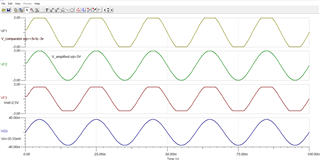
I am using the TLV9062 op-amp in my application to amplify a small signal (30mV) from a Zero-Phase Current Transformer (ZCT) to around 3V. I also plan to use the second op-amp as a comparator to compare the amplified signal with a reference voltage before sending it to a microcontroller.
Are there any reference designs, application notes, or design calculation guides available for the TLV9062 in such an application? Specifically, I am looking for:
I would appreciate any documentation or example circuits related to this.
Thanks!
Hello Sampath, welcome to the TI e2e forums.
1) Designing Gain and Offset in Thirty Seconds
2) I am not aware of any specific concerns other than Vos may grow a little bit wider.
3) High temperature and large input difference cause some Vos shift. Hysteresis gives more noise immunity.
Hi,
As mentioned previously, I am using the TLV9062 for signal amplification and comparison in my design, with a 3V supply. My comparator reference voltage is set to 2.5V, and I am getting the expected output. However, I have some concerns regarding the comparator output and alternative op-amps.
Looking forward to your expert guidance.
Sampath,
Will this output be suitable for direct interfacing with a microcontroller GPIO?
No, it is not good.
Is this design sufficient for hardware prototyping?
The design is not ready yet. Supply is 6V, that is a little too high for TLV9062. What is microcontroller voltage? Do you have access to both ZCT leads, in other words, do one side have to be grounded?
I see two outputs, VF2 linear and VF1 non linear. Do you plan to use both outputs or just the final digital output?
In any case give me the math equation(s) for output(s).
1.Supply is 6V, that is a little too high for TLV9062 & What is microcontroller voltage?
I am using a 3V supply for the TLV9062 in my design. However, in the simulation, I assigned separate power supplies for each op-amp. I made a mistake by setting the comparator stage supply to 5V instead of 3V, whereas in the actual hardware, both op-amps will operate from the same 3V supply.
Microcontroller voltage is 3.25V.
2.Do you have access to both ZCT leads, in other words, do one side have to be grounded?
I am using the MR-1 ZCT. Yes, I have access to both ZCT leads, and the ZCT is grounded in my design.
3.I see two outputs, VF2 linear and VF1 non linear. Do you plan to use both outputs or just the final digital output?
I am using only the final digital output to the MCU, and for verification purposes, I have checked the amplified output in simulation.
[Is there a method to obtain a comparator output of 3V to 0V instead?]
4.In any case give me the math equation(s) for output(s)
Amplified Output (VF2):
VF2 = (1 + Rf / Rin) * VZCT
VF2 = (1 + 82.3kΩ / 1kΩ) * 35.55mV
VF2 = 3V
Reference Voltage:
Vref = (R2 / (R1 + R2)) * Vsupply
Vref = (5kΩ / (1kΩ + 5kΩ)) * 3V
Vref = 2.5V
Sampath,
One thing I noticed is that that is no burden resistor for the current transformer. I think there should be one.
For the final digital output, should this represent current of a greater than certain magnitude or zero current crossing time?
Hi,
1.One thing I noticed is that that is no burden resistor for the current transformer. I think there should be one.
After placing the burden resistor, I am getting 35.55mV, which I have directly applied as an AC source. The amplified output is obtained correctly; however, in the comparator stage, the output is swinging between +3V and -3V.
2.For the final digital output, should this represent current of a greater than certain magnitude or zero current crossing time?
The final digital output represents fault current detection by indicating when the current exceeds a set threshold. It does not detect zero current crossing time.
3.Is there any other method to achieve a 3V to 0V output? Also, for hardware design, are there any additional factors to consider?
Sampath,
Here is a lightly tested solution. LM393LV open drain comparator. For single channel, try TL331LV or TL393LV
R1 (and supply voltage) sets over current detect threshold. The VF1 voltage.
D1, D2, R2, R3 are over voltage protection, ESD/EOS
100k can be a weak pullup of the GPIO.
GPIO pulses low for over current (positive side looking only) ; uC should have a pin interrupt capability (so you don't have to watch or latch the over current detection)