This thread has been locked.

If you have a related question, please click the "Ask a related question" button in the top right corner. The newly created question will be automatically linked to this question.

INA333: Dual axis strain gauge layout recommendation

Part Number: INA333
Other Parts Discussed in Thread: REF3318

Tool/software:


Hello,


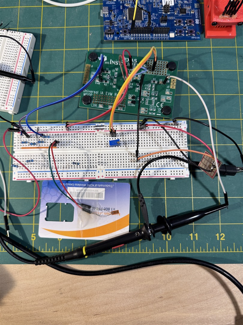
I am designing a battery powered product that needs simultaneous dual-axis strain gauge measurements, and am having some difficulty with the design.  Board VDD is 3.3, though I've boosted to 3.6 for the INA333 and added a 1.8V LDO for vref.  The strain gauge resistance is nominal 350 ohms, +/- 2 ohms for its operational range, and I'm using a quarter wheatstone bridge as input to the INA333.  Readings are using a 12 bit ADC with a somewhat selectable input range from 0-3.3V.  Accuracy and variations due to temperature will be handled in post processing using calibration data.

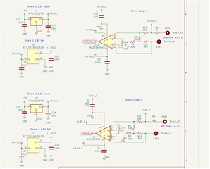
(note, in the above schematic, VDD is boosted to +5V, but I would prefer not to if I can avoid it)

When I assemble a single axis circuit on a breadboard, it behaves more or less as expected, but when I put two of them side by side, the readings, VO seems to be pegged to VDD, and I am suspecting that having two wheatstone bridges next to each other is just causing a resistor network nightmare.

Is there a recommended way to do this sort of thing, or  a different part that would be more appropriate?

Thanks,

--

Neil

  • Hey Neil,

    Could there have been an error in implementation? I don't see why proximity between the two circuits would cause any sort of interference. There aren't really any high frequency components, and strain gauges typically are slow-changing. As an aside, I don't believe you need two separate REF3318 devices (or HT7136), you should be able to supply both INA333's REF pins with a single REF3318 and single HT7136 for the supply.

    Do you have a picture of your setup so that I may provide a second set of eyes to check?

    Best,
    Gerasimos

  • Hey Gerasimos,

    There definitely could be implementation errors (and I'm hoping this is the problem).  I just can't seem to find the issue.

    Thanks for the confirmation on dual power rails.  At the time I was thinking that power isolation was the answer, but sadly, not so much.

    I assume by 'setup' you mean my breadboard - I'll rebuild it and send a pic.

    --
    Neil

  • Hey Neil,

    Correct. Thank you for taking the time to rebuild the breadboard.

    Looking forward to your response!

    Best,
    Gerasimos

  • Hey Gerasimos,

    Here's what I'm looking at now.   This setup works...sort of.  I am finding it difficult to get a VO centered around 1.8V when I increase the gain to the point where I can see reasonable variation on the scope when moving the strain gauge.  I need quite a bit of gain to see much of anything, but when I increase it, the quiescent V0 just gets closer and closer to 0V (or VDD if I swap V+ and V-) , and my variance is < 1V.  I can deal with that if I have to, but I don't understand why I am unable to keep the output near Vref.

    In the picture:

    - VDD is 3.6V

    - The 3 resistors are 1% 360 Ohm.

    - The little protoboard off to the side is the 1.8V LDO for Vref

    - The pot in the middle is connected to Rg 

    - The series resistor in line with the strain gauge is 10 ohm

    --
    Neil

  • Hey Neil,

    So my first thought here is that the Rg node is very sensitive to parasitic capacitance and can be prone to errors if the Rg is not very tightly set. From the datasheet, as little as several picofarads of capacitance on Rg can be enough to destabilize the INA333. For a prototype, I wouldn't be terribly worried about gain error or other over temperature errors, I would probably just focus on stable operation of the device first.

    If you want to prototype a variable resistor on Rg, I would probably solder the pot directly to the pads at Rg, and remove any other connections to Rg besides the pot.

    Best,
    Gerasimos.

  • Hey Gerasimos,

    Ok, thanks for the suggestions. 

    I was able to fiddle with the resistor values to get some output that looks good - a reasonable spread centered around 1.8V.  I'm worried about transferring those values to a PCBA though.  This is essentially what I did last time, and when the boards came back, nothing worked properly when I isolated the INA333 and strain gauge parts of the boards.  Still certainly possible that I made some errors when laying out the boards and choosing components, but I'd like to avoid that happening again if I can.  Do you have any layout suggestions?

    Thanks,

    --

    Neil

  • Hey Neil,

    For layout suggestions, I would recommend keeping a short path to Rg, and keep Rg on the same layer as the INA333 to minimize parasitics as much as possible. I would be mindful of the paths that the sensitive analog traces take, and look out for any opportunities for noise to couple onto the inputs of the INA333.

    Additionally, when adjusting resistors in the circuit, did you try to simulate over resistor variance to check how this will affect the circuit? This can be done in PSpice for TI, which is a free simulator with many of TI's SPICE models pre-downloaded. Additionally, I would check the variation in common-mode over tolerance, to make sure you are still in a range that allows for maximum output swing. This can be done with the Analog Engineer's Calculator. If you would like an example project I can generate one for you as a template to go off of for your design.

    Also, if you would like to send your schematic/layout, we would be happy to review and provide feedback!

    Best,
    Gerasimos