This thread has been locked.

If you have a related question, please click the "Ask a related question" button in the top right corner. The newly created question will be automatically linked to this question.

INA250: INA250A4PWR uses bidirectional current? and all GND1, GND2, GND3 connects to negative rail not ground?

Part Number: INA250


Tool/software:

Question 1.

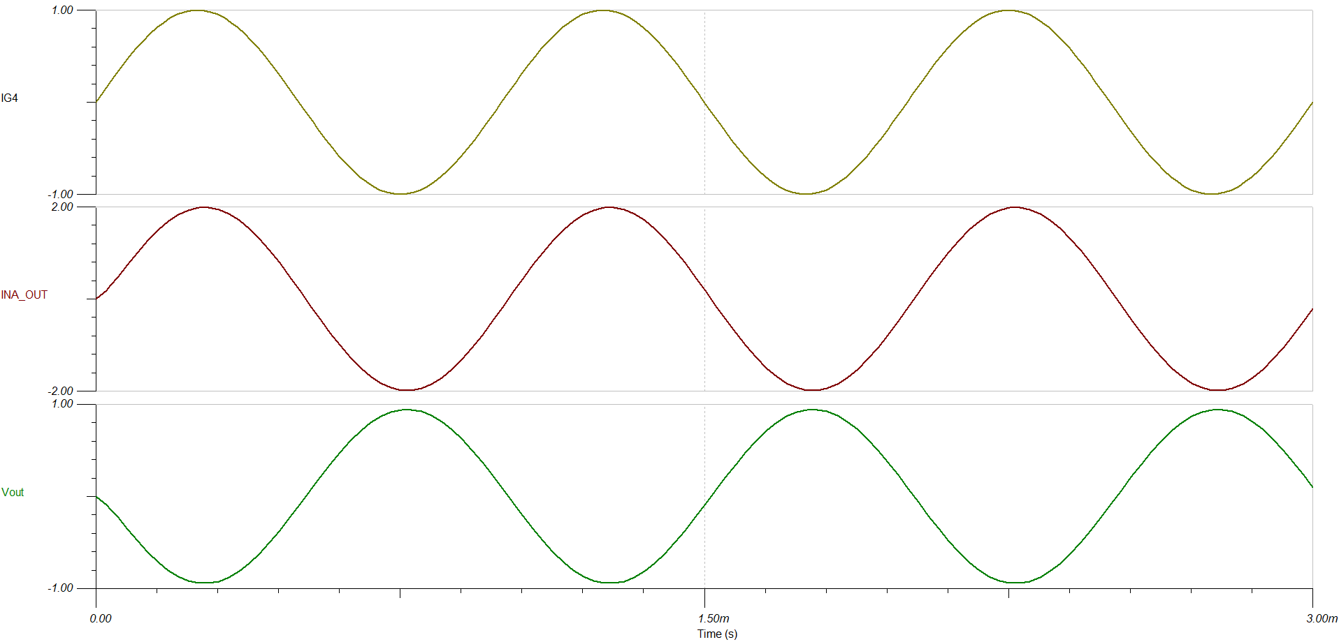
As you can see here I am using INA250A4PWR and OPA189IDBVT in the design. I would like to make sure the following circuit design would work for both positive and negative currents let’s say +1A and -1A (bidirectional) ? So per datasheet the gain OUT of  INA250A4PWR should be +2V or -2V based on the input. Please confirm.


Question 2.

In INA250A4PWR part, are the GND1, GND2, GND3 pins the VN (negative rail voltage) of the internal Op-Amp ?  As you can see I connected all those 3 GND pins to my -15V rail not to the GND. Please confirm.

  • Jak,

    Yes, you should be able to split the power supplies in this way to power the device. However, be aware that by referencing the GND node to -15V, the maximums of the device will also shift by this amount (ie, the recommended positive VCM of the device reduces to 21V, and the absolute maximum will reduce to 25V).  

  • Could you please answer my Question 1 and 2 above ? I specifically want to know if this device works with both positive and negative currents. Yes or No? 

    Also what is GND1, GND2 and GND3 pins in this device is that needs to be connected to ground or negative voltage rail for the op-amp ? In LTSpice simulation connecting those to ground is not working as it should. It works only when I connect to -15V.

    Thanks,

    Jak

  • Jak, 

    On question 1, yes, the device in bidirectional mode can support bidirectional current flow provided the VCM remains inside valid range, and yes. you are correct. A +/- 1A signal will result in a +2/-2V output on the INA output. I threw together a quick simulation of your schematic to demonstrate below:

    For question 2, there are 3 GND pins on the device (pins 6, 8, and 11), all of which must be referred to the same reference point. If you reference them to proper GND in the simulation, then the device will not be able to swing low on the negative ampacity, and will slam into the rail of the device. You would need to place the REF pin at a voltage high enough to allow the swing in both directions, such as mid-supply. Is referencing the simulation to GND causing improper response, or causing the simulation to break?

    sbom964.TSC