Part Number: OPA549
Tool/software:
Hi,
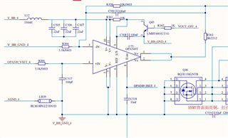
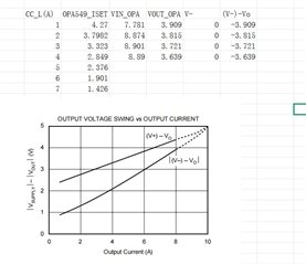
Plesae check our OPA549 schematic diagram, why our OPA549_ISET is only about 4.3A and the VIN_OPA is more than 7A, thanks.
This thread has been locked.
If you have a related question, please click the "Ask a related question" button in the top right corner. The newly created question will be automatically linked to this question.
Part Number: OPA549
Tool/software:
Hi,
Plesae check our OPA549 schematic diagram, why our OPA549_ISET is only about 4.3A and the VIN_OPA is more than 7A, thanks.


Hi Zhang,
What is VIN_OPA in this schematic? Is this OPA549_VSET_4?
What is your V+ connection?
You have implemented your current limit circuitry correctly, but it is important to remember that the current limit is only used in instances where the amplifier is exiting linear operation.
Is this a voltage controlled voltage source?
This circuit looks to have a DC gain of 1+ (10k/5.1k)
The interesting thing is that I see your output is changing as ILim is changing. This means the amp is wanting more output current.
The figure you sow is actually the claw curve. This can depend on ILim, but as we discussed earlier, ILim should only be activated during non-linear operation.
What is connected to the output of the OPA549?
Thanks,
Jacob
Hi Jacob,
1. The VIN_OPA is the input voltage(The V_BB pin);
2. The V+ is connect to Buckboost and it can be regulation voltaget;
3. The change in output voltage is due to the fact that the reverse current is set to 5V while our source is set to 4V.
At this time, the reverse current flows back through the lower tube of the OPA. As the voltage sampling point is located at the back,
there is impedance in the path, resulting in loss from the output of the operational amplifier to the port output.
Hi Zhang,
I think I understand now. You want to know why BB is consuming 7A and OPA I set is only at 4.3A, Correct?
What is the efficiency of your buck-boost converter?
Can you measure the current flowing into the V+ pin?
Thanks,
Jacob
Hi,
Please refer to below waveform:
1. The direct reverse injection testing, the PIN3 is red line and the PIN4 is the blue line:

2. Fixed the PIN4 voltage to 1.384V, the output voltage is 3.99V:

3. Fixed the buck boost voltage to 9V, the red line become thicker and the blue line lift up:

4. The schmeatic diagram:

5. We need to know why the amplifer stable forward current output is 7A max. and the stable reverse current output is only 4A,
and the current waveform is oscillated when the output current more than 4A, thanks.
Hi Zhang,
Thanks for the additional information. I see there is some additional capacitors on the circuit which I had not seen before. Is there anything after these capacitors which connect to U39 output?
Figure 1 is confusing. Why change pin 4 voltage as triangle wave, is this desired? Is pin 4 set by feedback somewhere, or fixed value?

Figure 2 has oscillations up to 4V. We should not see oscillation. This is likely a stability problem. Can you increase C262 value until no more oscillations appear?

Amplifier has open-loop output impedance change with Iout. Negative current may make the OPA unstable in certain scenarios. Increasing C262 may help stabilize the OPA. If this is not enough stability, it may be necessary to reduce size of C263
Thank you,
Jacob