This thread has been locked.

If you have a related question, please click the "Ask a related question" button in the top right corner. The newly created question will be automatically linked to this question.

OPA541: Output Distortion of Improved Howland pump

Part Number: OPA541
Other Parts Discussed in Thread: INA240, OPA551, OPA548, OPA593, ALM2403-Q1, OPA2991, OPA596

Tool/software:

Hi,

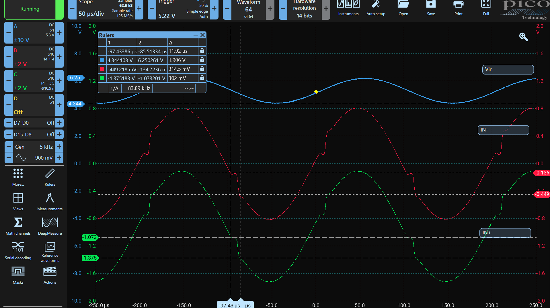
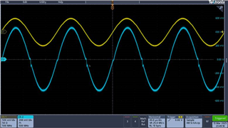
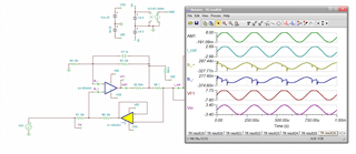
I am using OPA541 in an improved howland pump to drive a coil. The coil parameters are R = 0.68 , L = 16 uH. 

I am seeing output distortion when the frequency of Vin is above 1kHz. The circuit and the waveforms are below. 

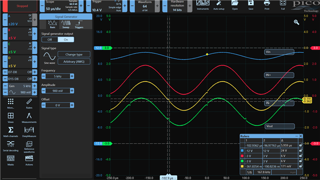
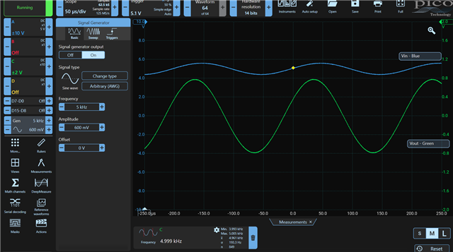
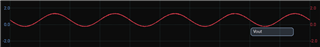
When I add a DC offset to the Vin the distortion is gone but the output is no longer centered around 0. Am I using a correct method to get rid of the distortion or is there another recommended technique .

  • Hi Gautam,

    This is strange to see. 

    Can you also probe IN+ of the OPA541 and IN- of the OPA541? This may help offer some insight as for why this is happening. 

    Do you mind sharing your TINA schematic? I can check to see if there is anything abnormal in SPICE. 

    Thanks,

    Jacob

  • Hi Jacob,

    Thank you for your reply. I have probed IN+ and IN- and attached the screen shot below. I have also attached the Tina file below. I have noticed that to remove the distortion, the given DC offset value is not the same as yesterday. 

    Without DC offset

    with DC offset. 

    OPA541_v1.TSC

  • Hi Gautam,

    Thank you for your great help in probing these traces. 

    I can see that there is an unexpected abnormality at IN+ and IN-. Since the Howland current pump provides negative and positive feedback, it can be challenging to isolate where this abnormality is occurring.

    I assume VS1 and VS4 are just used for TINA testing, correct?

    What I can state with high certainty:

    1. This should not be a lack of swing to rail for either power amplifier. 

    2. The INA240 should not be able to disrupt the control loop for the Howland current pump. 

    3. This should not be a common mode limitation of either amplifier.

    I am wondering if this is some byproduct of the current changing direction out of phase of the voltage, and causing the RC snubber to activate (R5 and C2)

    Did you determine this snubber circuit to be necessary in your application? 

    Could you try to lower the capacitor value and or increase the resistor sizing to see if the distortion decreases?

    Thank you,

    Jacob

  • Hi Jacob, 

    Yes VS1 and VS4 for simulation. I have tried without the snubber in the circuit and with a resistive load of 4 ohm. I have also tried using the subber resistance R5 as the load as shown in the figure below.

    With resistive load, the distortion is not as significant but still exists. Could it be due to the layout?

  • Hi Gautam,

    Thanks for testing the experiment without inductance or capacitive snubber.  

    It is interesting to hear that you still see the distortion even with these components removed. 

    This could possibly be layout related. This looks like some non-linear change in impedance to me. Maybe ground shift on the board. Maybe the load GND is changing from the large current flowing into the GND plane. 

    The strange thing is in that we still have this being solved by adding common mode voltage, right?

    Maybe this is something related to GND currents. Does the signal frequency change this distortion? 

    Maybe we could change the load resistor to see if this is related to output voltage or output current. 

    Thanks,

    Jacob

  • Hi Jacob,

    Yes, the problem seems to go away with adding a common mode voltage. One thing I forgot to mention is while adding this DC bias, the supply current is no longer symmetrical between Vs+ and Vs-. Vs+ is around 1A while Vs- is around 11mA for an input signal of 800mV.

    Below are the waveforms at different loads (4ohms and 10 ohms)

    Vin - 200mV , f - 10 kHz , R_L = 4 ohms

    Vin - 200mV , f - 10 kHz, R_L = 10 ohms

    What I have observed is the distortion increases with frequency and load.

  • Hi Gautam,

    Thank you for your patience as we continue to debug this issue. 

    This is very helpful to see more evidence of this distortion. 

    I think of it this way: it seems that the distortion is occurring when the device is encountering large rate of change on the output with heavy load current. 

    Are you using decoupling capacitors close to the supply pins of the device? Perhaps the inductance in the supply trace is limiting the rate at which dynamic current can be applied to the device VCC/VEE pin. https://e2e.ti.com/blogs_/archives/b/precisionhub/posts/the-decoupling-capacitor-is-it-really-necessary

    Your detail regarding the imbalance in supply current makes sense. This is indicating that the device is only sourcing current into the load connected to GND when we DC bias the input. Perhaps the VEE connection has too large of inductance to run with no DC bias.

    Is the load directly on the PCB? 

    Thanks,

    Jacob

  • Hi Jacob, 

    Thank you for your help so far. No the load is not on the PCB. It's is a magnetic shield at least a meter away.

  • I understand. What does this signal travel on? Is this cable inductance represented by the L1 inductor?

    Best,

    Jacob

  • I am using a coax cabel (141-0.5MSM). I have measure the total inductance of the coil along with the connecting wires it comes to R = 0.6 L = 16.05uH. 

    I forgot to answer one of the pervious questions. Yes I am using decoupling caps close to the supply pins. 

    To give more information on the board. It is a 4 layer board with 

    Top - Signal/GND

    L1 - GND

    L2 - Power plane (+25V/ -25V)

    Bottom - GND

  • Your PCB stack up is exactly what I typically recommend. The issue is not decoupling caps then. 

    So the INA240 is on the same PCB as the Howland current pump, correct? You then connect the SMA cable to whatever load you want to use for the current forcing. The resistive testing you did before, was this with or without the coax cable before the resistive load?

    I have thought this through a bit more, and I can make some more definitive statements:

    The only way IN+ of the OPA541 could see this "blip" is from the OPA551 positive feedback. 

    This is actually quite interesting because it suggests that the OPA541 is actually following the instructions of the OPA551 exactly as it should.

    The important question is in regards to how and why this blip is forming. Is this being created by the OPA541 or the OPA551.

    I do not know how common mode would really change any of this as the OPA's should not really care where the common mode voltage is set at. 

    I do have a rough test which may help us understand if the load is causing the OPA541 to blip, or if the positive feedback of the OPA551 is introducing the distortion. 

    If you remove R6, you will now disconnect the positive feedback from the Howland current pump.

    This turns the circuit into a voltage controlled voltage source which has a series output resistor (forces current through the coil)

    Maybe this could be an easy way to test what exactly could be causing this blip. 

    Please let me know what you think.

    Thanks,

    Jacob

  • Hi Jacob, 

    That is correct, INA240 is on the same pcb as the howland pump.

    The resistive load is with the coax cable. I used one of the coax cables with the other end cut and used phoneix connector to connect to a power resistor. 

    One this point I have seen the same distortion with just the snubber resistor R5 (located on the pcb) acting as the load. 

    That is a good idea, I will try removing R6 and see if the distortions are still present tomorrow. 

    Regards,

    Gautam Modumudi.

  • Hi Jacob,

    I ran the test with R6 removed.

    The distortion still exists but at lower levels. 

    The distortion goes away with a common mode voltage just as in the previous case. 

    I checked with only R5 acting as a load (ie a Resistive load) and the distortion still exists. So this leads me to believe that OPA541 is the one causing the distortion.  

    I also checked by increasing the feedback cap C4 to 22pF and distortion still exists. 

    Just to verify, I soldered OPA551 on a bare board, and it works as expected. There is no distortion. 

    Ran another test with OPA541 configured just as a voltage follower as shown below.

    Distortion does still occur.

    It is not as pronounced at lower frequency. 

    Regards,

    Gautam Modumudi.

  • Gautam,

    You have taken great data here. I completely agree with your summary that this distortion is coming from the OPA541.

    I do not have OPA541 samples on hand, but I am working with our planning team to have these units sent to me for bench confirmation. 

    I have similar family OPA54x power amps on hand which I am working to test today. I have been in contact with some of the Engineers who are more familiar with these series of power amplifiers, and I have come to learn that the OPA541 has especially observable output crossover distortion (not to be confused with input crossover distortion). I am told that this was an inherent characteristic of the class AB output stage for this device which varies with load current and frequency. Interestingly, it seems the Burr-Brown Engineers did this in attempt to save power when outputting low current near mid-supply. 

    Increasing your common mode voltage helps fix this problem as you are not engaging the high current sink driver. 

    Here is a similar E2E thread which I had not seen before: https://e2e.ti.com/support/amplifiers-group/amplifiers/f/amplifiers-forum/1003478/opa541-distortion-at-the-bottom-of-output-waveform?tisearch=e2e-sitesearch&keymatch=opa541#

    I am sorry you are encountering this undesired characteristic with this OPA. I have never seen output crossover distortion this bad. 

    What are your requirements for the power amplifier? Does this distortion prevent the circuit from operating? 

    Thanks,

    Jacob

  • Hi Jacob,

    The power amplifier needs to output maximum of 3A.

    the load is a B1 coil of a NMR field. Because of that it cannot have any DC offset. Also for this the operating current is between (100mA-3A) depending on the field required.

    I will go through that post and see what solutions they have provided. But from a brief glance it looks like doing a redesign as a composite amplifier is looking like the solution. 

    Looking forward to your test results and see if they match up.

    Regards,

    Gautam 

  • Yes, composite may be the best way, though I would like to prove this out before I send you down the path of being a guinea pig with this device.

    I spoke with a senior Engineer, and he says this is fully related to output distortion, and there are no simple ways to solve this problem.

    I see, no DC offset makes sense for your application. 

    Will send over the data on Monday. I only had a little bit of time with the OPA548 in lab.

    Best,

    Jacob

  • Hi Gautam,

    Sorry for my delayed response. 

    The composite amplifier idea will unfortunately not work here due to the crossover distortion effectively being a time delay problem. 

    No matter how much AOL I add with a composite amp, I will be unable to change the behavior of the output stage. 

    I shifted towards analyzing alternative solutions with alternative product selections. 

    I was able to test the OPA548 in lab, and the data is unfortunately still suffering from similar distortion effects. This device appears to not have any distortion at light loads, but seems to pick up similar distortion artifacts around 100mA. 

    I was able to find that a solution exists for this problem, it just unfortunately does not exist at this very moment. 

    We are releasing a next generation device like OPA541, just on a modern process technology with improved specs across the board. 

    This device was able to drive 3A with no distortion effects, though this device is unfortunately not available just yet. This device will APL in June of this year and fully RTM in October. 

    What is the project timeline here?

    Best,

    Jacob

  • Hi Jacob,

    Thank you for your help so far. 

    I was reading the other thread on OPA541 distortion and saw a method to bias the opamp into class A with a power resistor between Vout and Vs-.


    The output waveform does not have any distortion up to 600mV input. I was using a 33 ohm power resistor consuming 0.7A of current. This might be one way to solve the issue at the expense of efficiency. 

    If you already have the circuit for a composite amplifier setup, would you be able to test it out with a resistor tying Vout to Vs-. 

    My project timeline is around mid-April. 

    Regards,

    Gautam Modumudi. 

  • Hi Gautam,

    Thanks for taking the data with the 33 ohm resistor.

    Yes, if the extra power consumption can be tolerated, then we can force the output into class A operation with a resistor from OUT to V-.

    Funny enough, the OPA548 model matches the output distortion I see with the bench test:

    Simulated without V- resistor:

    Simulated with 10Ohm V- resistor:

    OPA548_v1.TSC

    Bench test +-1.1A load, no VEE resistor.

    Bench test +-1.1A load, with 10Ohm VEE resistor.

    These measurements were done without the composite amp structure, but I will be testing that next. 

    I am still playing around with the model to better understand how the composite amplifier in voltage controlled voltage mode compares to the Howland pump in voltage controlled current mode. 

    This looks like a viable option so long as we are happy with the additional power consumption.

    Best,

    Jacob

  • Thank you Jacob for all the testing. I did not see any distortion in the OPA541 TINA model. It is interesting that OPA548 shows the distortion. 

    It is fine to have additional power consumption. The project is not battery operated so power consumption will not be the issue. 

    Regards,

    Gautam Modumudi.

  • Hey Gautam,

    Great to hear that power is not a problem here. 

    Yeah, it is interesting and unfortunate that the OPA541 does not have this behavior modeled. 

    As I understand, your first measurements show how the device can still drive small negative output currents without suffering from the output crossover distortion:

    Assuming this to be true, I believe something like a 5-6ohm resistor to VEE should give you enough current to force the OPA541 into exclusive class A operation even at 3A load current. 

    In my simulations, this seems to work outside of the fact that the model is only giving me 8A current limit instead of 10A limit. 

    Do you happen to have any lower value power resistors/the ability to parallel more of the 33ohm resistors? I am thinking you may be able to at least confirm this operation without spinning the board. 

    Best,

    Jacob

  • Hi Jacob,

    The first measurement without any distortion as shown in the picture is with a DC offset to the input signal. 

    I placed an order for 5 and 10 ohm power resistors. I will test with them as soon as they arrive. 

    Regards,

    Gautam Modumudi.  

  • Hi Gautam,

    Yes, that is correct. The first measurements were with the additional DC offset. 

    Perfect! Please let me know how things go.

    Thanks,

    Jacob

  • Hi Jacob,

    I ran the tests with tie-down resistor of 20ohm. The output waveform 'decays' after a minute or so. I have attached a short screen recording below. 

    Blue - Vin

    Green - Vout

    The supply current on +25V starts decreasing once the output waveform changes. 

    I measured the temperature of the IC. It reached a maximum of 60C.

    My current limit resistor is 150mohm.

    Is this the effect of reaching the thermal limit?

    Regards,

    Gautam Modumudi.

  • Hi Gautam,

    Thanks for throwing the device on bench with the new resistor. This video is very helpful to me. 

    Yes, this is a bi-product of the thermal limit activating. the thermal limit is running real time, and reacts to the active die temperature in attempts to maintain safe operation.

    A majority of power dissipation occurs from the voltage drop in the output stage transistor. It may be worthwhile to experiment and see if V+ can be reduced any to help reduce power consumption in the device. 

    Are you able to use a larger heatsink, or reduce VCC? Reducing VCC would be the easiest way to improve power efficiency, but I know some applications have fixed supply rails. 

    60C case temp can easily be much higher internal die temp, especially for a device which is outputting a time domain signal (variable power with respect to time)

    Remember, we will have significantly more power loss the further that the output is forced from the V+ rail. If we are able to reduce V+ a bit, we will certainly see less thermal effects. 

    What heatsink are you currently using?

    Thanks,

    Jacob

  • Hi Jacob,

    I am using this heatsink with a 19CFM fan and an SIL thermal sheet between the heat sink and the OPA541. I will try with a lower VCC and check the results. .

    Regards,

    Gautam Modumudi.

  • Thanks Gautam! 

    That heatsink looks sufficiently sized for the application. I am hoping reducing VCC will get us in the range for where we need to be. 

    Best,

    Jacob

  • Hi Jacob,

    I tried playing with the Vcc and R_pulldown values. The maximum output I could get out of the device is 1A @ 10kHz before distortions or thermal limiting starting acting up. This is far from my original design specifications [3A @45kHz (max)].

    I would conclude this topic at this as I don't see a way around it. 

    My one question is in composite amplifier configuration is the bias current lower required lower?

    Regards,

    Gautam Modumudil. 

  • Hi Gautam,

    I am sorry to hear that we are not able to find a pulldown value which allows for functionality without overheating. I was really hoping that this method could solve our distortion issue. 

    I am disappointed that this output crossover distortion is something which somehow goes completely unmentioned in the datasheet. I am currently working on content to hopefully better explain the architecture reasons for why this occurs on our Burr-Brown power amps. 

    It does seem that output crossover distortion has effectively been eliminated in all of our new products. It is just a shame that our new 10A device is outside your design window. 45kHz at 3A is relatively easy for this device to achieve (I tested this in lab to verify that I do not see any distortion effects).

    There still are some ways to realize a solution today if you are still interested in some of our options.

    One of which would involve utilizing a discrete push-pull output stage using power transistors, and an op-amp. 

    Alternatively, it could also be possible to parallel power amplifiers together to create higher current drive. Paralleling can work well, but this also introduces some additional complexity in the design of the system. This article shows what this can look like for a different power amp (OPA593):

    https://www.ti.com/lit/ab/sboa553a/sboa553a.pdf?ts=1742320134081&ref_url=https%253A%252F%252Fwww.google.com%252F

    I have extra EVM's for some of our smaller power amps. If you want, I would be happy to test the parallel configuration on bench to see if this is possible for your application requirements. 

    Regarding your question, yes a composite structure can reduce the effective bias current of the power amplifier. This assumes that the high bandwidth amplifier is less IIB than the power amp, but this is very possible to be in the single digit pA range for IIB for CMOS high speed amps. This is one of the nice advantages to using the composite structure. The unfortunate problem here is in that more Vid/more AOL will not fix the inherent problem that the OPA541 has. 

    Thanks,

    Jacob

  • Hi Jacob,

    Thank you for all your help. My next plan was to use design the output push-pull stage with discrete mosfets. 

    If you already have the answers which of the power opamps have the least distortions? I could try that in parallel configuration to see if it meets my design requirements. 

    Regards,

    Gautam Modumudi. 

  • Hi Gautam, 

    Yes, discrete push-pull may be the best option. It is still possible that this discrete design will have some crossover distortion, but it should be possible to reduce this distortion via the addition of series diodes before the output transistor. This method can help ease the Class A transition to Class B.

    The ALM240x family of devices are specifically optimized to drive resolvers with very low distortion at relatively high currents. These devices however typically output only ~500-750mA per channel. I can spend some time with this device in lab to see what the performance looks like for your application. This design would require at least 3x/4x ALM2402F (dual amplifier) in parallel configuration to reach your 3A requirement. 

    I am taking a few days off later this week, but I should be able to test this Monday if that timeline is okay with you. 

    Thanks,

    Jacob

  • Hi Jacob,

    I will go with a push-pull output drive option over paralleling opamps. So there is no reason to prioritize testing that in the lab. 

    Thank you for all your help. Have a good vacation.

    Regards,

    Gautam Modumudi.

  • Thanks Gautam,

    Please let me know how the discrete output stage development goes. I am happy to offer help if needed.

    Thanks,

    Jacob

  • Will do! Cheers!

  • Hi Jacob,

    Hope you had a good vacation. I have the initial design for the push-pull output stage with ALM2403. Wanted to have a sanity check before I do the PCB layout and test the device. 

    Regards,

    Gautam Modumudi. 

    ClassAB.zip

  • Hi Gautam,

    Thanks, it was a nice to pick up a quick vacation!

    The design is looking good architecturally. 

    The ECX10x20 FET's seem like a great fit here for the required current drive. 

    It is also good to see a low current path in the transistor network, this should help reduce crossover distortion. 

    D1 and D2  diodes are a nice protection feature for the output stage. Z1 and Z2 are great to see as well. 

    I did make a slight mistake in advising the ALM2403-Q1. While this device is very low distortion, it is only a 24V supply device. I did not factor in such a large Vout wave driving the external transistor circuit, so it will be necessary to use a higher voltage device. 

    If you can use a +-20V or +-18V supply rail, something like the OPA2991 may work well for you. 

    If you need to use a +-27V or +-24V rail, something like 2x OPA593 devices may work well for you. The OPA596 is another good option, but this device will not RTM for a few more months. 

    Outside of the change in OPA, everything else looks good to me.

    I simulated the AC response of your circuit with OPA2991, and you are plenty stable with about 78 degrees of phase margin:

    Please let me know what you decide for the OPA selection. 

    Thanks,

    Jacob

  • Hi Jacob,

    Thanks for the feedback. I realized too ALM2403 only has a max of +/13V after I uploaded the files. I was planning on using OPA551 as I have seen it has no output distortions. I will check out OPA2991. I'll post updates once I have the pcb and finished testing it. 

    Regards,

    Gautam Modumudi.

  • Hey Gautam, 

    Great to hear that the design is moving ahead!

    OPA551 is perfectly fine to use as well. 

    Thanks,

    Jacob