Part Number: OPA695
Tool/software:
Hi,
I am working on a new PCB version using the OPA695IDBVR and I would like some PCB advises.
Generally on my current design the amplifier stage is working wellI but when my design has troubles it is always due to an OPA695 failure.
I have no idea why it is like that and I would like to solve it in my new PCB version.
I use the OPA695 as an inverting amplifier, our standard resistor couple is 402R / 200R for an amplification of 2. We sometime increase the amplification up to 6 with a couple 402R/68R.
The signal to amplify is between 200MHz - 1GHz.
I use a non balance power supply. +8V / -3V. Could it be a source of problem? I have readen some element about that.
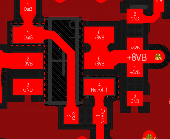
I have a 4 layers PCB and the PCB design has no polygon cutout on the different layers under the component. It also has no cutout for pins IN+ / IN- / OUTPUT. Is it ok for you?

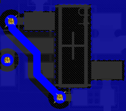
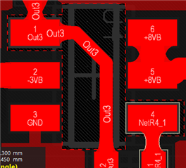
I plan to add cutout on all the layers under the component. Do you think it is a good idea to trace the feedback net under the pin? Do you recommend me to go throught vias to connect the feedback resistor to the output?

Thank you in advance for your help,
Best regards