This thread has been locked.

If you have a related question, please click the "Ask a related question" button in the top right corner. The newly created question will be automatically linked to this question.

PGA309: Temp PGA Common Mode Input Range

Part Number: PGA309

Tool/software:

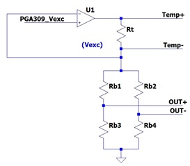
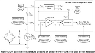
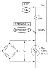
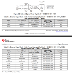
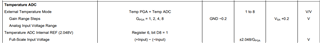
I'm planning on implementing temperature sensing and bridge excitation per this schematic. This will allow my bridge common mode voltage to remain roughly centered about VEXC/2 so that I can take advantage of the input PGA's high gain (128) while taking into account the Coarse Offset DAC's limited range (~±60 mV). I would connect Temp+ to the TEMPIN input and use VEXC for both the Temp ADC Input Mux and Temp ADC Reference. Looking at figure 2-20 of the User's Guide (Rev C), it appears that the Temp PGA gain is performed after the differential voltage is determined. I.e., with a gain of 8x, it seems OK with 2.747V and 2.9V at the Temp PGA inputs. I want to confirm if this is accurate or if I would need to use an external difference amp and lower the common-mode temperature voltage closer to ground.

  • Hello Brandon, 

    Figure 2-20 is accurate, and the intended circuit will also work as long as the inputs to the PGA309 (VIN1 and VIN2) labeled in block diagram as "OUT+" and "OUT-" are within the input common mode voltage range of the PGA309 over the temperature range of the device. 

    As a summary Figure 2-20 is illustrating that RT (top side series temperature resistor) changes less with temperature (50ppm/C) than the entire bridge resistance (3500ppm/C) and therefore can be gained (TEMP PGA) and compared (TEMP ADC) to either VREF, VEXC, and VSA.

    In the block diagram configuration and in the example, it makes sense to compare to VEXC as the full-scale range. TEMP PGA has the option of gains 1, 2, 4, 8 - not only 8. 

    However, I do not believe this answers your question of input common-mode voltage range of the device. To answer this, I recommend using the PGA309 calculator available on the product page: 

    Using the calculator and your system's conditions, the calculated PGA settings are shown: 

    In the configuration shown in your block diagram, RT+ would be used: 

    Please let me know if you need additional clarification or I can always do the calculation for you if the application's temperature range is provided and what the expected resistance of your bridge is at those temperatures along with normalized sensor data. 

    All the best,
    Carolina 

  • I'm really only asking about the TEMPIN input. Maybe "common mode" isn't the right term. I need to know the absolute range of the input when using gains of 1, 2, 4, or 8 for the Temp PGA. For example, if my TEMPIN signal is 4.2V and VEXC is 4.1V and the Temp PGA gain is 8, will I get 800 mV at the Temp ADC, or will there be some issue with the Temp PGA because the inputs are wanting to be multiplied by 8 (~32V which would not be possible). Or, is everything OK because the Temp PGA is true difference amplifier (not an instrumentation amplifier) and the difference can be amplified in the presence of high common mode voltages? The fact that the datasheet says the temperature input can go ±0.2V beyond the supply rails implies a difference amplifier.

    The available tools don't help much with the Temp PGA or ADC. The PGA309 calculator doesn't show the internal, intermediate voltages for the temperature circuitry.

  • Hello Brandon, 

    Can you help me understand how TEMPin would ever be bigger than Vexc? 

    All the best,
    Carolina 

  • In my schematic, the low side of Rt is at the VEXC voltage; therefore, the high side of Rt will be at a higher voltage. I'm doing it this way to maintain the full VEXC voltage across the sensor bridge.

  • Hello Brandon, 

    Okay understood, the other linked e2e is making sense, thank you.

    The TEMP_PGA can be assumed to have an instrumentation amplifier topology in which the gain is first applied to the inputs and then the difference is taken, I would reference Figure 6-2 and Table 6-3 to help with your temperature calculations and expected digital output in Hex: 

    The ±0.2V is in reference to the ADC input which happens after the PGA output: 

    For the scenario you have outlined, I recommend using a gain of 1. 

    All the best,
    Carolina

  • Looking at Figure 6-2 and Table 6-3, along with Figure 2-20, it seems more likely that the gain is applied after the difference voltage. Otherwise, in Figure 2-20, the 8x gain would be applied to 2.9V and 2.747V. In Table 6-3 it shows an input of +5V. Is the instrumentation amplifier really useful with an input at the positive rail? Even at a gain of 1? It would be nice to see a real-world example like Figure 6-2 with a smaller input range (but still near the positive rail) and higher gain setting. A 0V to 5V swing on the Temperature signal isn't realistic, especially in the Figure 2-20 configuration.

    As far as the ±0.2V, how can the PGA output beyond the power rails? I feel like this is referring to the external pin. The specified range is in reference to the power rails whereas the rest of the Temperature ADC parameters are referring to the differential voltage from the Temp PGA outputs wrt the reference voltage. The datasheet also characterizes the Temperature input impedance in the MΩ range instead of input bias currents typically specified in instrumentation amplifier datasheets (or with impedances in the GΩ range). 

  • Hello Brandon, 

    I see where you are coming from. Okay let's assume it's the other way around (as seen in Figure 2-20), I can always measure it to verify. 
    Connect Vexc to 4.1V and TempIN to 4.2V and see if I can TEMP PGA (gain of 8) to read 800mV at the Temp ADC. 

    Any other TempINs you would like me try? & what is your intended REF for the ADC?

    All the best,
    Carolina 

  • Yeah. That seems like a good plan. Maybe even test something close to, - or even right at - the 5V power rail, just so we have more information on the total input voltage range. You may have to reduce the gain if you're applying something like 5V vs VEXC near 4V. I'm planning on using VEXC as my reference voltage because that would be the only way to cancel out its variability due to the linearity corrections.

    Thank you,

    -Brandon

  • Hello Brandon, 

    Understood, thanks for the confirmation. I expect to have lab results back to you by end of week, 3/21, Dallas Time. 

    Attached an excel with ideal values. TempADC.xlsx

    All the best,
    Carolina

  • Thanks again. Looking forward to the results. You may want to double-check your ideal expected digital values. It seems they were calculated using the ratio as the voltage. E.g., for the Gain=1 with a voltage of -0.1, I'd expect the counts to be FCE1. You have FF3D which corresponds to a voltage of -0.02439V.

  • Hello Brandon, 

    Thanks for letting me know, I'll make sure to double check my work. 

    All the best,
    Carolina

  • Hello Brandon, 

    Just giving you a quick update, that this has proven unexpectedly difficult using the EVM/software. I am still working on it. 

    All the best,
    Carolina

  • Hello Brandon, 

    You were correct in your interpretation of the PGA, the inputs are first subtracted and then gained up. 

    Attached is a excel in which I cover the values from the GUI, ideal and actual results for all of the gains. 
    I recommend a gain of 4 for the scenario you have outlined above, it utilizes 90% of the full-scale range of the ADC. 

    TempADC (1).xlsx

    I used a reference of 4.067 instead of the 4.1, for ease of experimentation, theory applies the same. 

    All the best,
    Carolina 

  • Thank you, Carolina. I think this answers all my questions and it's good to have the empirical evidence.