Tool/software:
I am following up from this E2E thread: https://e2e.ti.com/support/amplifiers-group/amplifiers/f/amplifiers-forum/1470875/pga280-what-is-the-minimum-and-maximum-time-delay-between-falling-edge-sclk-and-falling-edge-ecs_n-output-on-gpio
It's my customer asking these questions.
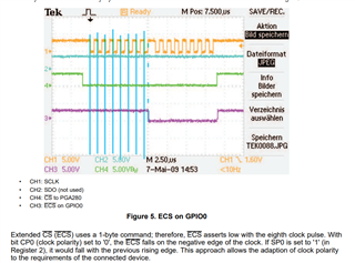
The PGA280 specification (SBOS487B-JUNE 2009-REVISED MARCH 2020, pg 24) indicates that CP0 =1 causes ECS_N to fall after the SCLK negative or falling edge (from section 7.4.1.1). The app note you linked in the previous post indicates that that CP0 =0 causes ECS_N to fall after the SCLK negative or falling edge (Figure 5).
Which document is correct? My customer wants to use the SCLK falling edge so should CPO be set to 0 or 1?
Also, figure 5 of the Application Note has the ECS_N set to be asserted on the rising edge of the SCLK. Do we have a better plot for the ECS_N that shows more accurate Tpd between the falling edge of SCLK and the assertion of ECS_N?