This thread has been locked.

If you have a related question, please click the "Ask a related question" button in the top right corner. The newly created question will be automatically linked to this question.

TLC27M2A: EMI/EMC ISSUE

Part Number: TLC27M2A
Other Parts Discussed in Thread: TLV9102

Tool/software:

Hi, 

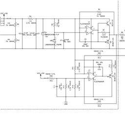
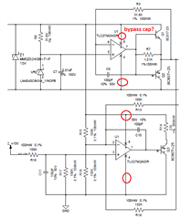
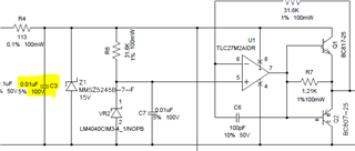
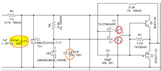
we are using TLC27M2AIDT in one of my applications. I have found an issue with it during CS test, at test voltage level of 10V, 150Khz to 80 Mhz, opamp output used to change its state during the test, same issue is observed in 4 tested boards.
also we have did an experiment by replacing opamp with similar characteristics from ST Microelectronics MPN: TS27M2AIDT. the previous observation is not repeated with this IC. i am not able to find the actual reason behind this. 
can you please help in finding the difference that is creating this issue


Thanks,
Mohan. 

  • What exactly do you mean with "CS"? Conducted susceptibility? You did not specify the measurement setup or the results, but I'd guess that the TLC27M2A uses very fine structures that have capacitive coupling between the inputs and outputs.

    The TLV9102 is EMI hardened; see section 7.3.1 of its datasheet.

  • Hi Mohan,

    I have found an issue with it during CS test, at test voltage level of 10V, 150Khz to 80 Mhz, opamp output used to change its state during the test, same issue is observed in 4 tested boards.

    As Clemens indicated, the Conducted immunity is a system level test. You are talking about the op amp that is only a part of an entire system. To conduct CS test, you have to monitor current at the power input line in a DUT, and how to you narrow down to an op amp in a system. Please explain how the CS test is conducted. 

    also we have did an experiment by replacing opamp with similar characteristics from ST Microelectronics MPN: TS27M2AIDT.

    What is the test result? Do you still see outage in your CS compliance. Where are the outages between 150kHz - 80MHz? I have a feeling that it may not be related to the op amp. Please let us know. 

    Best,

    Raymond

  • Hi Clemens, 

    Yes, it's conductive susceptibility testing as per EN/IEC 61000-4-6. Attached below block diagram for reference and its setup overview. the current reading in the ammeter is used to change for applied noise, even without a change in the load sense resistor current.

    also to add, this is only observed at 10V/m test level.

    When tested at 3V/m, its working as per expected functionality.

  • Hi Raymond, 

    Please find my response in the above thread.
    let me know if any information is required.


  • Hi Mohan,

    I do not know what compliance tests are conducted based on your description. 

    3V/m or 10V/m is the an electromagnetic field is generated for conducting Radiated Susceptibility test, where the EUT is exposed to it the field (radiating energy).

    CDN does not generate an RF field (not radiating energy) in V/m; CDN technique injects RF voltage into input cables. Please clarify your setup and the op amp detailed schematic (show me the actual schematic including op amp bias point and bypass capacitor etc.). 

    You can only conduct one test setup at a time, not both. Based on your setup, I could say that voltage regular may be the issues in you setup, why you think that TLC27M2AIDT is the issue, where the outages are. Is this switching or linear regulators. Please let me know. 

    Best,

    Raymond

  • Hi Raymond, 

    we are using electromagnetic clamp method for injecting noise into the lines, 

    Please clarify your setup and the op amp detailed schematic (show me the actual schematic including op amp bias point and bypass capacitor etc.)

    Unfortunately, the schematic cannot be shared due to the restricted availability.

    You can only conduct one test setup at a time, not both. Based on your setup, I could say that voltage regular may be the issues in you setup, why you think that TLC27M2AIDT is the issue, where the outages are. Is this switching or linear regulators. Please let me know. 

    we are testing it only on 24V dc line, not both . its a linear regulator which converts 24V to 10V dc to power opamp, voltage regulator we have changed multiple parts and tested still issue persists. when i have modified the opamp from TLC27M2AIDT to TS27M2AIDT, we havent found the issue.

    the difference in both parts observed from datasheet is TLC27M2AIDT has input clamping diodes where TS27M2AIDT doesnt have. also Common-Mode Input Voltage Range of TLC27M2AIDT extends below the negative rail, where as TS27M2AIDT ranges from 0V to Vcc.
    please help in finding out the differences if you find any. 


    Thanks,
    Mohan

  • Hi Mohan,

    the difference in both parts observed from datasheet is TLC27M2AIDT has input clamping diodes where TS27M2AIDT doesnt have.

    This makes some senses. A PCN has issues in 12/2023 due to FAB change in this part, see the PCN. 

    https://mm.digikey.com/Volume0/opasdata/d220001/medias/docus/5733/PCN20231130004.1.pdf

    Yes, it is likely that back to back input diode is designed into the this part, therefore, the input differential voltage should not exceed +/-0.5Vdc, and input common mode voltage is extended as well. If this is the case, you have to test the op amp according the new finding. Unfortunately, the datasheet is not updated in this regard, and I will ask the documentation team to release the update soon. 

    BTW, when the input differential voltage exceeds the absolute max. ratings, the part could be damaged as well. If you are able to send me the op amp schematic, I can take a look.  

    Best,

    Raymond

  • HI Raymond,

    Please find the opamp circuit. for your reference.


    This makes some senses. A PCN has issues in 12/2023 due to FAB change in this part, see the

    does a FAB change can be the cause of this issues.?

    Yes, it is likely that back to back input diode is designed into the this part, therefore, the input differential voltage should not exceed +/-0.5Vdc, and input

    is there any impact with the diodes added

    Please help with your inputs.

    Thanks,
    Mohan

  • Hi Mohan, 

    I do not see the required bypass caps in the supply rails. If this is single supply rail, then you need one 0.1uF bypass cap minimum per op amp. If the op amp configurations are with dual supplies, two 0.1uF minimum on each supply rail is required. 

    At the beginning of the query, you mentioned that this is one amp test configuration. The latest schematic is shown that an entire product is undergone CS testing. 

    is there any impact with the diodes added

    Back to back diodes should not cause the CS failures. Many op amps have designed with back to back didoes at the input and it is used to protect the op amp's, which it is used to protect the gate oxide from breakdown in CMOS device. Many op amps have the type of input topology, even some of BJT op amp is using the back to back diode topology. 

    when i have modified the opamp from TLC27M2AIDT to TS27M2AIDT, we havent found the issue.

    Could you elaborate the modification a bit? Is the injected RF signal coupled through input signal or coupled into op amp via op amp's power rail? What is the failure? I need to some details here in order to understand the failure mechanism. 

    Best,

    Raymond

  • Hi Raymond,

    I do not see the required bypass caps in the supply rails. If this is single supply rail, then you need one 0.1uF bypass cap minimum per op amp. If the op amp configurations are with dual supplies, two 0.1uF minimum on each supply rail is required. 

    an 10nF, 50V rated 0603 ceramic capacitor is placed at input of the opamp, which was not show in in the circuit. attached the image below, which is placed near the opamp supply pin 8 in the PCB layout.

    At the beginning of the query, you mentioned that this is one amp test configuration. The latest schematic is shown that an entire product is undergone CS testing. 

    yeah, i might have missed to convey it in an elaborative way.

    Could you elaborate the modification a bit? Is the injected RF signal coupled through input signal or coupled into op amp via op amp's power rail? What is the failure? I need to some details here in order to understand the failure mechanism

    RF coupled noise is injected on the 24 VDC lines, which will power up the module, and 24 VDC is converted into 10 VDC using an linear regulator(LM317LBDR) for supplying power to opamp.

    during the CS test at 10V test voltage level applied, we are seeing the current variations in the 24VDC lines, where expected is to be constant.(we will monitor the loop current of 24VDC for our applications, where the opamp will drives the currents based on its sense input voltages)
    so i have tried testing replacing multiple components and verified, and found while replacing opamp, earlier seen current variations are not observed.
    so we came to an conclusion that issue is with opamp.
    after the test is stopped, the part intends to work as expected, it doesnt fail. only during injection of noise it behaves differently compared with the other. 
    also to add, TI part with test voltage level of 3V, its behaves normal, no current variations are observed as seen with 10V test level, only at 10V test level, current variations in 24VDC are seen.


    Thanks,
    Mohan


  • Hi Mohan,

    an 10nF, 50V rated 0603 ceramic capacitor is placed at input of the opamp, which was not show in in the circuit. attached the image below, which is placed near the opamp supply pin 8 in the PCB layout.

    Please place 100nF or 1uF low ESR capacitor next to pin8 supply rail (assume single supply rail). Near the op amp supply pin8 will not help and the value is too low. Please try it and let me know. 0.1uF is the minimum requirement to decouple the high frequency to GND at the pin8.  It is not clear how you passed the previous CDN without the decoupling capacitor. 

    during the CS test at 10V test voltage level applied, we are seeing the current variations in the 24VDC lines, where expected is to be constant.

    The zener diode has parasitic capacitance. At high frequency, the parasitic capacitance becomes dominant and the Vref is unable to clamp the voltage properly. I would increase C7 and C3 to low ESR 1uF (may be 2.2uF) in order to decouple the high frequency. Without the stable Vref at the U1, the V-I current conversion is not going to work properly.  

    Please let me know if you have additional questions. 

    Best,

    Raymond