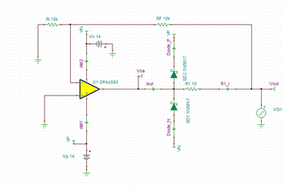
This thread has been locked.

If you have a related question, please click the "Ask a related question" button in the top right corner. The newly created question will be automatically linked to this question.

OPA593: Absolute Maximum Ratings

Part Number: OPA593
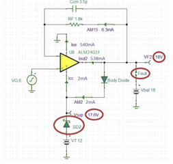
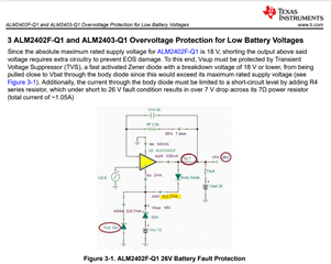
Other Parts Discussed in Thread: ALM2402F-Q1

Tool/software:

Hi,

The condition of OPA593 are as follows.
V+=+14V , V-=-14V , E/D=Enable.

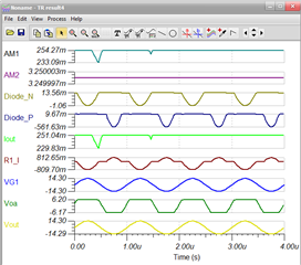
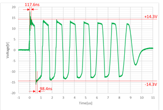
If OUT pin exceed 14.3V during 117.6ns , is OPA593 safe ?

Out pin Voltage in lightning surge test  is shown in Figure.

Is there a time regulation about Absolute Maximum Ratings?


Best regards

  • Hello Takahiro-san,

    You are correct, abs max should be maintained at all times.

    There is a time element to overstress, and hundreds of ns is considered somewhat short. Since it is hard to predict the exact balance between overstress time, and over-voltage, we do not specify abs max with any reference to time. 

    There is an important detail needed here, is your positive supply rail capable of sinking current? If not, it may be necessary to install a Schottky diode for blocking voltages higher than 14V from appearing at the connection to the V+ supply. 

    Here is a great article which covers over-voltage events for resolver drivers (very similar to OPA593): Overvoltage Protection of Resolver-Based Circuits

    Generally speaking, it may be possible for the device to survive this overstress event just by nature of the short time element of the condition. To be safe, I would at least consider installing the Schottky diode on both supply rails. It may also be beneficial to install external protection diodes on the output of the device, connecting to each supply rail. 

    This diagram accurately shows the conduction path during over-stress event:

    So long as the current flowing through the internal body diode is less than 10mA, you do not need external output diodes to V+ and V-. If the supply rails can both source and sink current, then the Schottky diodes will also not be needed. 

    Note, these diodes have very few downsides. If you have space on the board, it may be nice to place the component pads on just in case this is determined to be necessary. 

    Please let me know if you have any questions. 

    Thanks,

    Jacob

  • Hello Jacob-san,

    Thank you for replying.

    I read article Overvoltage Protection of Resolver-Based Circuits .

    The supply rails can both source and sink current.

    Is it possible to pass a current 250mA through the internal body diode of OPA593 output FET, as in the ALM2402F-Q1?

    If the internal body diode of OPA593 output FET pass a current more 250mA , Is it necessary to install external protection diodes on the output of the device, connecting to each supply rail? or more 10mA?

    Best regards

    Takahiro

  • Hello Takahiro-san,

    Thank you for the additional details. If the supply rail can source and sink current, then this is good for the design.

    Yes, the next concern is this body diode. This body diode should ideally not conduct more than 10mA for OPA593. It can tolerate some higher currents, but this is not typically recommended.

    I like the idea of external protection diodes to the VS+ and VS- rail. 

    I can create a simulation to demonstrate the design if it offers help to you.

    Thanks,

    Jacob

  • Hello Jacob-san

    I understand body diode limitation current.

    "I can create a simulation to demonstrate the design if it offers help to you."

    ->I want to see simulation circuit. Could you please provide it?

    Best regards,

    Takahiro

  • Hi Takahiro-san,

    Here is a simulation which demonstrates the current steering through the use of Schottky didoes on the output rail.  

    I intentionally use a 14.3V 1MHz sine wave at "Vout" to simulate the lightning stress test. 

    OPA593_OVP.TSC

    Here, we see that the diode P and diode N work to protect the output of the amplifier, preventing any over-voltage from appearing at the output of the op amp. 

    It is possible to reduce the value of R1 if you would like less voltage drop across this resistor during normal operation. 

    Please let me know if you have any questions. 

    Best,

    Jacob

  • Hello Jacob-san

    Thank you for simulation details and your advice.

    I will consider it.

    Best regards,

    Takahiro