This thread has been locked.

If you have a related question, please click the "Ask a related question" button in the top right corner. The newly created question will be automatically linked to this question.

OPA855: output bias

Part Number: OPA855
Other Parts Discussed in Thread: OPA856,

Tool/software:

https://www.ti.com/product/ko-kr/OPA855#design-tools-simulation

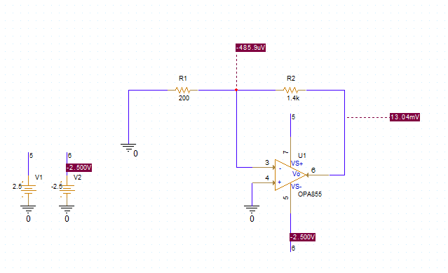
Hello. I built a simple inverting amplifier using the OPA855 for my circuit. However, I'm noticing that the output bias is clearly abnormal. As far as I know, the output should be around 0 V. I applied the PSpice model from the link above. When I run the same simulation using other amplifiers like the OPA856 or OPAx277 with the same configuration, the output appears normal. I would appreciate it if you could help me understand why this is happening.


******************************************************************************

NODE VOLTAGE NODE VOLTAGE NODE VOLTAGE NODE VOLTAGE


( 5) 5.0000 ( -5) -5.0000 (X_U1.ZO) 5.0000

(N1081188) 9.0866 (N1081198) 11.6510

(N1083154) 9.0866 (X_U1.MID) 3.3257

(X_U1.CMRR) 3.3256 (X_U1.ESDN) 9.0866

(X_U1.ESDP) 18.07E-06 (X_U1.CLAMP) 3.3256

(X_U1.PSRRN) 3.3250 (X_U1.PSRRP) 3.3252

(X_U1.VCC_B) -5.0000 (X_U1.VEE_B) 11.6510

(X_U1.VIMON) -118.8300 (X_U1.AOLNET) 3.8257

(X_U1.N06456) 18.07E-06 (X_U1.N10561) 68.07E-06

(X_U1.N10570) 35.03E-06 (X_U1.N11984) 35.03E-06

(X_U1.N11991) 9.0866 (X_U1.N25816) 314.3E-06

(X_U1.N28602) 12.7510 (X_U1.N30136) -5.4000

(X_U1.N30913) 314.3E-06 (X_U1.N31014) 314.3E-06

(X_U1.N35675) -8.4000 (X_U1.N35813) -8.4000

(X_U1.N38050) 15.0510 (X_U1.N38096) 15.0510

(X_U1.VOUT_S) 5.0000 (X_U1.X_U1.3) 0.0000

(X_U1.X_U1.4) 0.0000 (X_U1.X_U1.5) 0.0000

(X_U1.X_U1.6) 0.0000 (X_U1.X_U1.7) .8338

(X_U1.X_U1.8) .8338 (X_U1.N110431) -118.8300

(X_U1.N112292) 5.0000 (X_U1.N317950) 3.3257

(X_U1.N406634) -5.0000 (X_U1.N406794) 11.6510

(X_U1.N749288)-381.9E-06 (X_U1.VCC_CLP) -8.4000

(X_U1.VEE_CLP) 15.0510 (X_U1.X_E_N.3) 0.0000

(X_U1.X_E_N.4) 0.0000 (X_U1.X_E_N.5) 0.0000

(X_U1.X_E_N.6) 0.0000 (X_U1.X_E_N.7) .8338

(X_U1.X_E_N.8) .8338 (X_U1.N1254860) -149.2800

(X_U1.N1446199) 3.3256 (X_U1.N1446217) 3.3256

(X_U1.N1461236) 3.7147 (X_U1.N1461246) 3.3257

(X_U1.N1461252) 3.3147 (X_U1.N1481243) 9.2862

(X_U1.N1481253) 3.3261 (X_U1.N1481259) 3.3242

(X_U1.N1483677) -9.8109 (X_U1.N1483687) 3.3250

(X_U1.N1483693) 3.3411 (X_U1.N1483703) 3.3264

(X_U1.N1483713) 3.3102 (X_U1.N1490067) 3.3252

(X_U1.N1492098) .8142 (X_U1.N1492108) 1.6514

(X_U1.N1492118) 1.6514 (X_U1.N1492126) 1.6514

(X_U1.N1492376) 1.6514 (X_U1.N1534615) -39.4290

(X_U1.N1534625) 1.8280 (X_U1.N1534635) 1.8280

(X_U1.N1534645) 1.8280 (X_U1.N1534887) 1.8280

(X_U1.N1541593) -34.9180 (X_U1.N1541603) 1.9861

(X_U1.X_I_NP1.3) 0.0000 (X_U1.X_I_NP1.4) 0.0000

(X_U1.X_I_NP1.5) 0.0000 (X_U1.X_I_NP1.6) 0.0000

(X_U1.X_I_NP1.7) .8338 (X_U1.X_I_NP1.8) .8338

(X_U1.X_VOS_VS_VCM.1)-381.9E-06


VOLTAGE SOURCE CURRENTS
NAME CURRENT

V_V1 -1.891E-01
V_V2 -1.873E-01
X_U1.V_VCM_MAX 8.726E-09
X_U1.V_VCM_MIN -9.426E-09
X_U1.X_H3.VH_H3 1.222E-01
X_U1.X_VOS_VS_VCM.V1 1.399E-18

TOTAL POWER DISSIPATION 1.88E+00 WATTS

  • Hi Na,

    An observation that I saw in your circuit is-

    • The total supply (Vs+ - Vs-) for your circuit is 10V which is beyond the acceptable range of 3.3 to 5.25V (From datasheet). I would recommend to use a supply of +/- 2.5V if you want to bias the output at 0V.

    Few questions from my side-

    • What is desired output signal swing and DC bias?
    • What is the input voltage swing? 2mVpp?

    Regards,
    Aditya Gosavi

  • Thank you for your response.

    1. I overlooked the voltage range to be applied — since the circuit will use +5V or -5V, I’ve corrected the input voltage to +5V and 0V.

    2. I don’t expect a specific bias. But theoretically it should be 0V, so if it's close to that (around 50mV or lower), that would be acceptable.

    However, the output bias is still strange. It's showing 8.48V, which is very abnormal. Also, since the gain is 1.4k / 0.2 = 7 V/V, the output signal should be 7 times larger, but that’s not happening.
    The only thing that seems to be working properly is that the signal is inverted.

  • Hi Na,

    As you may know, op-amps have output headroom limitations, meaning they cannot drive the output all the way to the supply rails. Based on 5, 0V supply, the output can swing only from 1V to 4V in case of OPA855 (from datasheet page 7). Therefore, achieving a true 0V DC output in this configuration can be challenging. To address this I would like to suggest a couple of approaches:

    1. Midpoint biasing- To maintain the op-amp within its linear operating range with your current 5V and 0V supply, biasing the output at the midpoint (around 2.5V) would be advisable. This would allow for symmetrical signal swings within the output headroom.
    2. Dual supply-  Alternatively, using a +/- 2.5V dual supply would enable you to achieve a 0V DC output bias, as it provides a wider output swing range. This would allow the op-amp to operate within its linear range for a 0V output.

    To better understand the cause of the 8.48V output, could you please provide your circuit schematic file? Once I have the schematic, I can analyze the circuit and provide a more specific and accurate solution.

    Regards,
    Aditya Gosavi

  • What I truly intended was not a 0V bias, but to bias the circuit at a specific level. However, the values turned out to be quite different from what I expected. After looking into it, it seems this particular component might be the issue. Since the other components are working fine, I suspect there might be a problem with the PSpice model of this component. I’ve sent you a zip file of the circuit via direct message. I sincerely appreciate your review of it.

  • Hi Na,

    I looked into the PSpice Model for the OPA855 component in your schematic and I found a few differences with the PSpice Model that is on ti.com product page.

    I would recommend you to download the OPA855 Unencrypted PSpice Model Package: https://www.ti.com/lit/zip/sbomb43 from the product page, and use this component in your schematic, or edit the PSpice Model of your current schematic.

    I ran a DC simulation to check the voltages, and I saw appropriate values (+/-2.5V Dual Supply)-

    Let me know if you face any issues.

    Regards,
    Aditya Gosavi