This thread has been locked.

If you have a related question, please click the "Ask a related question" button in the top right corner. The newly created question will be automatically linked to this question.

INA281: Output from OUT pin

Part Number: INA281


Tool/software:

Hi All,


I have a question about the INA281.

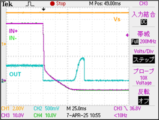
After the voltage on IN+ and IN- drops, a voltage is output to the OUT pin.

Why does this happen?

Best Regards,
Ishiwata

  • Hi Ishiwata,

    The common mode voltage you have shown here is outside of our recommended operating conditions and we do not guarantee functionality of the device outside of these conditions. However, the device will not be damaged unless the VCM goes below -20V.

    BR,

    Holly

  • Hi Holly,


    I apologize for the late reply.
    I appreciate your response.

    I have two questions about the INA281A.

    Could you please answer them?

    (1) When both the INA281A input pins IN+ and IN- are in a high impedance state with respect to GND, is it possible that the voltage of these pins will drop to about -8V?

    (2) If the answer to the above question is YES, is it possible that the balance of the bias currents of IN+ and IN- will be lost during the process in which both IN+ and IN- transition to a voltage of -8V, resulting in a voltage of several 100mV being generated at the output?


    Let me explain the background to these questions.
    I have previously asked this question and it was answered that the potential of the IN+ and IN- pins will never fall below GND as long as the INA281A is used with a single power supply.

    The circuit I am currently using has a FET on the high side of the current sense resistor, which controls the power supply on/off.
    In addition, there is a diode between the current sense resistor and the load to prevent backflow.

    When I simulated this circuit using PSPCIE for TI, the voltage at IN+ and IN- was -8V when the FET was OFF.
    From this, I assume that there is a charge pump circuit inside the IC, and that when IN+ and IN- are in a high impedance state to the common mode, they are biased to around -8V. Is this correct?

    In customer testing, a pulse signal of several hundred mV was observed several tens of milliseconds after the FET was turned off. (The waveform shown in the previous post.)

    To identify the cause, I have come up with a hypothesis.
    As the IN+ and IN- pins transition to -8V, a difference occurs in the bias current of both pins.
    I think that this is converted into a voltage by the 1.2kΩ resistor installed for filtering, and even though no current is flowing through the current sense resistor, a high voltage is generated at the output pin.
    This is not reproduced in simulation.
    Is my hypothesis correct?


    Best Regards,
    Ishiwata

  • Hi Ishiwata,

    What is the sense voltage during this condition?

    What do you mean by the input pins are in a high impedance state with respect to ground?

    You 1.2kOhm resistors for filtering are very big. Section 7.1.2 of the DS talks about input filtering and recommends these resistors be no greater than 10Ohms. I would recommend referring to that section as it explains how these resistors can cause a mismatch in input bias currents.

    As far as the voltage becoming -8V let me look into this and get back to you.

    BR,

    Holly

  • Hi Holly,

    Thank you for your support.

    I will respond to your inquiry.


    What is the sense voltage during this condition?
     =>When I simulated the circuit, I observed 32 mV between IN+ and IN- during the FET was on.
      Using the real device, I observed about 500 mV on output if INA281A output during the FET was on.
      It estimates 25 mV of the input voltage.


    What do you mean by the input pins are in a high impedance state with respect to ground?
     =>When the FET is off, the impedance between the power supply and the sense resister is high, may be the order of Mega ohm.
      In the meantime, the impedance between the sense resister and GND through the diode and the load is quite high (may be the
      order of Mega ohm), as long as IN+ and IN- pins are biased bellow GND, due to the diode.


    You 1.2kOhm resistors for filtering are very big. Section 7.1.2 of the DS talks about input filtering and recommends these resistors be
    no greater than 10Ohms. I would recommend referring to that section as it explains how these resistors can cause a mismatch in input bias currents.
     => Thank you for your sound advice. I will follow your suggestion.

    As far as the voltage becoming -8V let me look into this and get back to you.
     =>Looking forward to get your answer.


    Best Regards,
    Ishiwata

  • Ishiwata,

    I can't say whether or not this is true:

    From this, I assume that there is a charge pump circuit inside the IC, and that when IN+ and IN- are in a high impedance state to the common mode, they are biased to around -8V. Is this correct?

    However, I think there is merit to your hypothesis and I suspect that if you reduce the input filter resistors this should help with the unexpected output as your VCM drops. 

    But again, this -8V VCM violates recommended operating conditions so I can not say with certainty whether that will or will not fix this issue.

    It would be recommended that you put these pins in a known state within operating spec when they are unused.

    BR,

    Holly

  • Holly,

    Thank you for your support.
    I have asked the customer to make the filter resistance less than 10 ohms.
    I am currently waiting for customer feedback.

    Best Regards,
    Ishiwata

  • Ishiwata,

    Thanks for the question and using the E2E forum.

    We are out of the office due to the U.S. holiday but will respond to your question when we return to the office Monday, 4/21.