This thread has been locked.

If you have a related question, please click the "Ask a related question" button in the top right corner. The newly created question will be automatically linked to this question.

OPA4202: Rectified wave offset

Part Number: OPA4202


Tool/software:

Hello,

Something strange is happening in my circuit and I would like to know if anyone can see where the problem is.

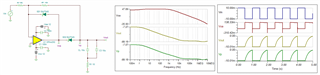
My circuit is as follows:

At the input would go a sine wave centered at 0, is separated into a positive and a negative rectifier, where we filter them to have a DC signal, and finally the two sides are subtracted.

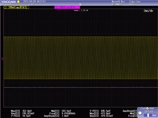
When the input sine wave has a frequency lower than 3 KHz, the operation is as it was planned, example of the operation in the following image.

We put a 958 Hz sine wave at the input and observe it with the yellow color, and the pink color at the node where components C11, C17, R10, R8 and D3 are connected:

But when we put high frequencies at the input, the capacitor is charged more than what is at the input, so there is a permanent offset.

Example of a 9.41 KHz sine wave looking at the same points.

Why does this offset occur in the capacitors and how can I stop it from appearing?

  • Hi Sosa, 

    Why does this offset occur in the capacitors and how can I stop it from appearing?

    Do you need to place the snubber at the output of the op amps? If the input is sinusoidal waveform, then the snubber circuit is not needed. 

    The snubber circuit is 20uF in series with 10ohm resistor and the dampened the input circuit near 958Hz. Also, I am not sure that the circuit will be stable without oscillation while driving this much capacitive load without op amp compensation. 

    Best,

    Raymond

  • Hi Raymond, 

    Thanks for replying.

    Sorry, the input doesn't have to be sinusoidal, it can be any shape.

    How can I check the stability of my circuit?

    Regards,

    Iván

  • Hi Iván,

    The circuit seems to be stable, but I am not sure what you are trying to get out of circuit. The circuit does not have much BW due to the heavy snubber dampen circuit. 

    OPA4202 E2E 04102025.TSC

    Here is Schottky diode forward biased simulation. 

    The loop analysis is shown that it has approx. 65 degree (180 - 114.52) of phase margin, which is stable.  When I performed the small signal step analysis, there is some overshoot, but it is not oscillating. I think that you should remove your snubber circuit or change to lower RC time constant, because it is killing the BW of the circuit. That is why you see that your scope shot is nearly attenuated in pink. 

    if you have other questions, please let me know. 

    Best,

    Raymond

  • Hi Raymond,

    Thank you for everything. The circuit works as a peak detector, which results in a lower operating frequency.

    It's more of a filter than a true snubber.

    Best regards,
    Iván