This thread has been locked.

If you have a related question, please click the "Ask a related question" button in the top right corner. The newly created question will be automatically linked to this question.

PGA281: usage with ADS1259 - desire schematic review

Part Number: PGA281
Other Parts Discussed in Thread: ADS1259, PGA855, PGA280, ADS127L11, ADS131E04

Tool/software:

Hello,

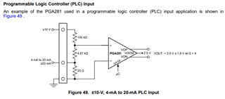
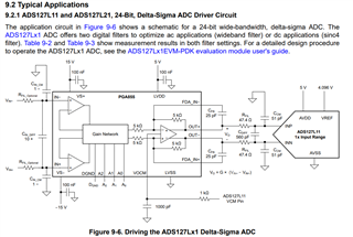
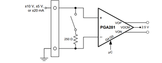
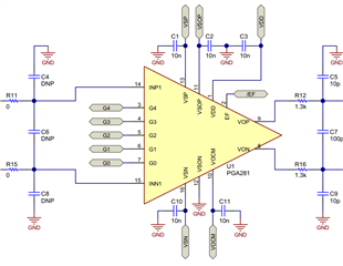
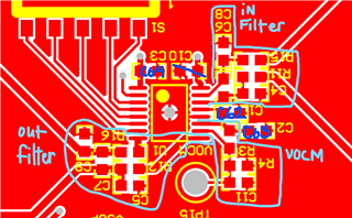
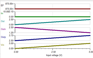
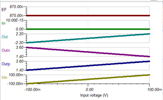
We are evaluating new design using FOUR sets of the PGA281+ADS1259 operating at +/-10V for variety of sensor applications.

We have a preliminary schematic and would like review/feedback - please contact me with email address to send PDF schematic.

  • Hello Mark, 

    Thanks for providing the schematic and sensor information through email, I will continue the support through this thread for continuity of support for the lifetime of the device. 

    Could you please provide what the voltages are at VSOP and VSON? I am assuming VSOP is 3.3V. 

    All the best,
    Carolina 

  • VSOP = 3.3V, VSON = AGND , VSP = +10V, VSN = -10V

  • Hi Mark, 

    1. Are there any additional power supply rails available in your system?
    2. I noticed the schematic shows PGA281 but you mention SPI signals. PGA280 is SPI compatible, PGA281 is gain select through GPIOs. Did you want to proceed with GPIOs? If so, I recommend upgrading to PGA855. 

    All the best,
    Carolina 

  • 1. Yes - we will also have 5VDC.

    Do we need different voltage(s)?

    2. We use SPI to the ADC and GPIO to PGA.

    Since we have 4 analog input circuits, we are concerned about noise interference if SPI is used to PGA, so we chose GPIO configuration.

    Is there an example schematic of the PGA855 used with the ADS1259?

    Our objective is to have 4 independent 24-bit analog inputs that can be configured differently and hopefully will not interfere with each other.

    Is there a better solution that what we have proposed?

  • Hello Mark,

    1. The voltage at the input pins has to be within ±2.5V of the supply rail: 


    Since the VSP/VSN are ±10V, and the input signal is ±10V, this doesn't allow enough headroom. 
    I recommend including higher voltage rails or reducing down the input signal as shown in the datasheet: 

    2. The gains on the PGA855 are a little bit more limited than PGA281, but the bandwidth is higher supporting up to 1MSPS.
    We do not have an example showing ADS1259, but we do have the ADS127L11 example, which is 24-bit Delta sigma device: 

    The input limitation will still apply. 

    I will continue to work on this on monday. 

    All the best,
    Carolina 

  • Hello Mark, 

    Thank you for your patience as I have had more time to work on this. 
    I have looked into the possibility of changing to PGA855 and ruled it out, as it cannot support 3.3V on the lower supply range.

    For all of the sensors, here are the constraints to design within (considering the schematic):

    • Input voltage range is (VSN) +2.5V to (VSP) - 2.5V -> -7.5V to 7.5V
    • Output swing from rail is typically 100mV, therefore (VSON) + 0.1V to (VSOP) - 0.1V -> 0.1V to 3.2V (centered around 2.5V - VOCM)
      • (Max output differential)/2 = Output Max - VOCM = 3.2V - 2.5V = 0.7V 
      • Max output differential = 0.7V * 2 = 1.4V 
    • Ensure internal nodes of the instrumentation amplifier are within the power supply rails (if this is violated, EF will go high). Recommend leveraging the following simulation: http://www.ti.com/en/download/aap/ReferenceDesigns/PGA281/PGA281_2TerminalPLCFig51.TSC

    Here are my recommended gains, expected inputs and outputs:

    Linear transducers: 

    Input Range VOP Range VON Range Output (VOP-VON) Recommended gain (G4:G0)
    -5V to 5V 1.88V to 3.12V 3.12V to 1.88V -1.25V to 1.25V 0.25 V/V (00001)
    0 to 5V 2.5V to 3.12V 2.5V to 1.88V 0 to 1.25V 0.25 V/V (00001)
    0 to 10V (if VSP is > 12.5V) 2.5V to 3.12V 2.5V to 1.88V 0 to 1.25V 0.125 V/V (00000)
    4-20mA w/140Ω (.56 to 2.8V) 2.64V to 3.2V 2.36V to 1.8V 0.28mV to 1.4V 0.5 V/V (00010)

    Loadcell:

    10V excitation * 2mV/V = 50mV span 
    Offset = 5% of span? = 12.5 mV (this is a guess, but the math still applies)

    0% -> 12.5mV, 100% -> 62.5 mV

    Input Range VOP Range VON Range Output (VOP-VON) Recommended gain (G4:G0)
    12.5mV to 62.5mV 2.64V to 3.19V 2.36V to 1.81V .275 to 1.38V 22 V/V (10111)

    Pressure transducer: 

    10V excitation * 10mV/V = 100mV span
    Offset = 1mV 

    0% -> 1mV, 100% -> 101mV

    Input Range VOP Range VON Range Output (VOP-VON) Recommended gain (G4:G0)
    1mV to 101mV 2.51V to 3.06V 2.49V to 1.94V 0.112 to 1.11V 11 V/V (10110)

    Displacement sensor: 

    10V excitation *4.2mV/V = 42mV 
    10V excitation * 9.6mV/V = 96mV

    Offset = 1mV

    Input Range VOP Range VON Range Output (VOP-VON) Recommended gain (G4:G0)
    1mV to 42mV 2.52V to 3.17V 2.48V to 1.83V 0.032 to 1.34V 32 V/V (01000)
    1mV to 96mV 2.5V to 3.03V 2.5V to 1.97V 0.011 to 1.06 11 V/V (10110)

    All the best,
    Carolina

  • Part Number: PGA281

    Tool/software:

    Questions - sorry for the delay - working on several issues at same time...

    1. Referring to the TINA file - are the 2.5K resistors (tied to 2.5V) needed?

    2. Should I run the interface between the PGA281<>ADS1259 @ 5V?

    3. Appears that in order to interface to the 10V sensor, we need minimum VSP=12.5V - then- what would VSN need?

  • Hi Mark, 

    I merged the two threads for simplicity. 

    1. Resistors are not required, VOCM is required. 

    2. Increasing the VSOP to be 5V will increase the output range of the PGA281 and will in turn increase the usable range of the ADC. If you would like I can redo my tables from above to reflect that. 

    3. Since the input is 0 to 10V, and the input voltage range of the device is (VSN) +2.5V to (VSP) - 2.5V, the minimum requirement is VSP = 12.5V, VSN = -2.5V. Leaving it at -10V is also fine. 

    All the best,
    Carolina

  • 2. Yes - we will run VSOP @ 5V, please update

    3. We will run VSP = +15V and since power supplies are usually symmetrical between positive<>negative outputs, VSN = -15V is likely - please update

  • Hi Mark,

    Caro is currently out of the office but will be returning tomorrow. If that changes I'll let you know and I'll need to receive the schematic from you to better follow what is happening in this E2E thread.

    Best Regards, 

    Robert Clifton  

  • Hi Mark, 

    Understood, here are the new values: 

    I am taking into account that the ADS1259 full scale range (VIN = AINP-AINN) = ±VREF = ±2.5V. 
    ADS1259 AVDD = 5V, AVSS = 0V
    Absolute input voltage range (AINP, AINN to DGND) = 0 to 5.1V

    Linear transducers: 

    Input Range VOP Range VON Range Output (VOP-VON) Recommended gain (G4:G0)
    -5V to 5V 1.25V to 3.75V 3.75V to 1.25V -2.5V to 2.5V 0.5 V/V (00010)
    0 to 5V 2.5V to 3.75V 2.5V to 1.25V 0 to 2.5V 0.5 V/V (00010)
    0 to 10V 2.5V to 3.75V 2.5V to 1.75V 0 to 2.5V 0.25 V/V (00001)
    4-20mA w/500Ω (2 to 10V) 2.75V to 3.75V 2.25V to 1.25V 0.5mV to 2.5V 0.25 V/V (00001)

    Loadcell:

    10V excitation * 2mV/V = 50mV span 
    Offset = 5% of span? = 12.5 mV (this is a guess, but the math still applies)

    0% -> 12.5mV, 100% -> 62.5 mV

    Input Range VOP Range VON Range Output (VOP-VON) Recommended gain (G4:G0)
    12.5mV to 62.5mV 2.7V to 3.5V 2.3V to 1.5V 0.400 to 2V 32 V/V (01000)

    Pressure transducer: 

    10V excitation * 10mV/V = 100mV span
    Offset = 1mV 

    0% -> 1mV, 100% -> 101mV

    Input Range VOP Range VON Range Output (VOP-VON) Recommended gain (G4:G0)
    1mV to 101mV 2.51V to 3.61V 2.49V to 1.39V 0.022 to 2.22V 22 V/V (10111)

    Displacement sensor: 

    10V excitation *4.2mV/V = 42mV 
    10V excitation * 9.6mV/V = 96mV

    Offset = 1mV

    Input Range VOP Range VON Range Output (VOP-VON) Recommended gain (G4:G0)
    1mV to 42mV 2.52V to 3.42V 2.48V to 1.58V 0.044 to 1.85V 44 V/V (11000)
    1mV to 96mV 2.5V to 3.56V 2.49V to 1.44V 0.022 to 2.11V 22 V/V (10111)

    All the best,
    Carolina

  • Thank you - will review these values...

    Additional question - could we use ADS131E04 in place of the 4X PGA+ADC ? (let me know if I need to start a new topic?)

  • Hi Mark, 

    I would open a new thread so that it may be assigned to the correct team.

    Looking at it quickly, I do not believe so as the gains offered by the ADS131E04 are 1, 2, 4, 8, 12 - the gains needed for your application are both higher and lower (attenuation) than that.

    It is possible a different integrated ADC could work. 

    All the best,
    Carolina

  • Hi Mark, 

    I saw that you emailed me with your final schematic and layout, sorry for the delay as I have been out of office this week. 

    I saw that you specify that the input ranges from ±100mV or 0 to 5V. Could you explain how the linear transducer does this for both voltage (0 to 10V) and current (4-20mA)? For the current are you implementing a resistor for C66? 

    All the best,
    Carolina

  • The linear transducer looks like a variable resistor – as the actuator moves the transducer, the voltage will swing between ground and positive rail, in our case, from 0V to 5V.


    The sensor outputs are -100mV to +100mV, in Wheatstone bridge configuration using -5VDC and +5VDC as excitation voltages.


    The key factors are;

    Minimum input voltage to the PGA is -100mV (on pin 15,  INN)

    Maximum input voltage to the PGA is 5V (on pin 14, INP)


    When linear transducer is used, “INN” will be grounded so the PGA is in single ended mode. INN=0V


    We are not operating in 4-20mA mode. There is other circuitry for that.

  • Hi Mark, 

    Understood, thank you for the clarification.

    I would make the following changes to schematic/layout: 

    • Add input common mode filtering options (seen by R11, R15, C4, C8) to be able to minimize common mode noise with the different sensors and the connector. 
    • Add output common mode filter options (C5 and C9 as DNP). 
    • Add a 10nF decoupling/bypass capacitor for VSN. 

    I reviewed your layout versus the EVM and it matches well, I would keep bypass capacitor placement & implement input filter shown in the top right-hand corner of the device: 

    C10 would be the decoupling/bypass capacitor for VSN, please place the cap near pin 16. 

    Output analysis: 

    Conditions: VSP = 10V, VSN = -5V, VSOP = 5V, VSON = 0V
    Taking into account that the ADS1259 full scale range (VIN = AINP-AINN) = ±VREF = ±2.5V. 
    ADS1259 AVDD = 5V, AVSS = 0V
    Absolute input voltage range (AINP, AINN to DGND) = 0 to 5.1V

    Input Range VOP Range VON Range Output (VOP-VON) Recommended gain (G4:G0) Sim Result % of ADC Full Scale Range
    0 to 5V 2.5V to 3.75V 2.5V to 1.25V 0V to 2.5V 0.5 V/V (00010)  50%
    -100mV to 100mV 1.4V to 3.6V 3.6V to 1.4V -2.2 to 2.2V 22 V/V (10111)  88%

    All the best,
    Carolina