This thread has been locked.

If you have a related question, please click the "Ask a related question" button in the top right corner. The newly created question will be automatically linked to this question.

INA592: Current Source and Current Sink Circuit

Part Number: INA592
Other Parts Discussed in Thread: XTR305

Tool/software:

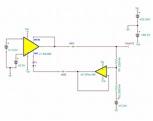
                                                               Fig1: Current Source Circuit

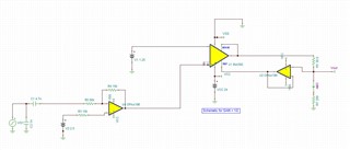
                                                     Fig2: Current Sink Circuit

Current Source Circuit (Source Mode): The circuit generates a current of 4-20mA when V2 is varied between 1.25V and 2.5V. I have successfully tested this in the TINA simulation and in practical experiments.

Current Sink Circuit (Sink Mode): The circuit is designed to produce a current of 4-20mA when V2 is varied from 0 to 1.25V. I obtained accurate results in the TINA simulation; however, I am not receiving the expected output in practical experiments, and also when i am trying to vary the V2 voltage it is not allowing to change and whatever voltage at V1 is appearing at V2(i.e 1.25).

Can you tell me what is the problem?

  • Doudu,

    In both cases, you will be violating the valid output range of the INA592. The output must be more than 220mV from either rail. For your sweep from 0-1.25V, the range from 1.2 to 1.25 will now be nonlinear.

    In your practical experiments, what are the values of the supply voltage and what is the voltage at the input, output and ref pins?

    Best,
    Gerasimos

  • Supply Voltage:24V

    Vin :0-2.5V

    INA592 IC  Vout = (V+ - V-)/2 = 0-62.5mV

    In Ckt Vout1/2 = Ref pin: Source Mode :0.25-5V , Sink Mode: 18V-23.75V

  • Previously TI Team told that output is Ok(Linear Region) and this circuit is suggested by TI

  • I given Bipolar supply of ±18V by this we are not violating the output limitation then also sink mode is not working

  • Hey Doudu,

    Can please provide where this circuit was recommended?

    The issue is when your load is terminated to the same V+ as your amplifier supply. Please see Figure 3-1 in the below application note. For a +/-25mA current supply, the load is not terminated to the same supply as your amplifier. Terminating your load to the same supply as the amplifier means that at low current the amplifier will have to drive the output to V+

    https://www.ti.com/lit/an/sboa437a/sboa437a.pdf

    Best,
    Gerasimos

  • The above circuit only i followed, i thought that there is no limitation on V_termination. In our product we will use the op amp supply and V_termination is same in case of Sink mode.

    In case of Source Mode the V_termiantion is connected to GND

  • Hello Doudu,

    The limitations of V_termination are not well discussed in the article. To output the lower range of currents, the output voltage will need to create a voltage differential across Rshunt. If Rload is terminated to V+, and 500uA needs to be dropped across Rs, then for 30.9Ω, a voltage difference of 15mV must be across Rs. This means that the amplifier will need to linearly be able to output V+ - 15mV, which the INA592 cannot do. Terminating the load to even 1 diode drop below V+ will allow sufficient output swing headroom to be able to drive lower currents.

    If you are trying to sink/source 4-20mA, would you be willing to consider one of the dedicated devices for this application? The XTR305 will sink or source 4-20mA

    https://www.ti.com/lit/ds/symlink/xtr305.pdf

    Best,
    Gerasimos

  • Hi Gerasimos

    I know XTR305 will serve my purpose but it's required bipolar supply of ±15V. which leads to cost and increase in PCB size .

  • For us 1-20mA ,this circuit works in linear region ok we won't go below 1mA. 

  • Hello Doudu,

    Understood, while the min supply of the XTR305 is 10V, and does not need symmetrical supplies, it does need a negative rail of at least -3V. I understand this may not work for you.

    1mA at 30.9 ohms of shunt resistance means that the amplifier will have to drop 30mV. To get into the linear output range of the INA592, the shunt resistor would have to be at least 220ohms to ensure robust performance. This will change the gain though, and you will need to have a different voltage input range.

    Best,
    Gerasimos

  • Hi Gerasimos,

    Now I tired with V- = 9.2, V+ =(0-18.4) ,Vcc =24V,Vss =GND,Rset =220 ohm , RL=250 ohm

    i am maintaining the 220mV for 1mA (INA will be in linear region)

    Source Mode(RL other end is connected to GND) :  when i varied V+ from 9.2 to 18.4 it is working fine

    Sink Mode(RL other end is connected to VCC) : In this case i should vary V+ from 9.2 to 0, but it is not allowing V+ to go below 1V. What could be the reason?

  • Hi Doudu,

    I am not very familiar with your circuit, so please forgive any misunderstanding on my side.

    You want to take differential voltage range and scale at 220mV/mA, creating a ~+-20mA current source, correct?

    If you want to sink current, you cannot have the negative rail of the INA be the same voltage as the load termination. 

    The current drive comes from the amplifier making a more negative voltage than the load termination. 

    Here is my sweep of your circuit with load terminating to GND (sourcing)

    Here is my sweep with load terminating to V+ (sinking):

    If you want both directions, you can connect load termination to mid-supply (12V):

    INA592_Current_Pump.TSC

    Was this a problem in simulation or real testing?

    Please let me know if you have any questions.

    Best,

    Jacob

  • Hi Jacob,

    I am taking about practical experiment(Please refer my previous conversation).

    First two graphs are ok for me but practically the sink mode is not working as expected. Thats what my query is.

    1.  I can terminate the load to VCC only not to midsupply (3rd simulation is not requied).

  • Hello Doudu,

    On the above schematic, can you please label the node voltages you are measuring on each node in your circuit?

    Please include VF1, VOUT1/2, IN+ IN- and IN+ of the op amp.

    I'm not sure I understand your issue from your description.

    Best,
    Gerasimos

  • My problem is resolved, by giving the input to INA592 using unity gain op-amp.

  • Hello Doudu,

    Was there some very low current limit on your supplies? The supplies will need to source a few mA to be able to drive the input to the correct voltage.

    Best,
    Gerasimos

  • Hi Gerasimos,

    Source Mode:                                                                                                        Sink Mode:

    I am using the attached final circuits, mentioning the power supply and input voltages.

    Vcc = 18V to 32V (Nominal is 24V) for all IC

    Vss = 0V

    VG1 = 500mV(HART Singal)

    V2 = 0-1.25V for Sink, 1.25 to 2.5 for Source

    V1 = 1.25V

    Loop Current =1 to 20mA

    can you please check any output voltage swing violation for INA592 and OPAx196 for both source and sinks modes from your side.


    Best Regards

    Vamshi

  • Hello Vamshi,

    This is the same setup as before, where I specified that the linear operation will be violated. You need to increase the value of the shunt resistor so that the output can drop enough voltage from rail to be within a linear output range.

    1mA at 30.9 ohms of shunt resistance means that the amplifier will have to drop 30mV. To get into the linear output range of the INA592, the shunt resistor would have to be at least 220ohms to ensure robust performance. This will change the gain though, and you will need to have a different voltage input range.

    Please make the changes to the shunt resistor and input voltage as specified earlier in the thread. As you have described the circuit, current below 7mA will not be able to be provided.

    Best,
    Gerasimos

  • Hi Gerasimos,

    The output voltage of INA Vout = Vref+g(V+ - V-) , where Vref  will Vref vary from 0.25Vto 5.25 in source Mode and 18.75 to 23.75 in Source Mode.

    So the Vout of INA is always greater than 0.25V it is in linear region only.

    I_out is not Vout/ 30.9  it is (Vout-Vref)/30.9

    Best Regards

    Vamshi

  • Hello Vamshi,

    For there to be a voltage differential across R1, there needs to be an output current from INA592. For there to be an output current, the output stage needs to be in a linear operating range.

    Let's look at just the source side. Below is a simple AB output stage. With no load, and the input trying to be 0V, the output can only go 1VBE above Vs-. This means that the lowest voltage the transistor can pull the output down to is 1VBE (usually 600mV) Any sort of load connected on this output to GND will have more drive strength than the amplifier output stage, and will pull the output to GND.

    Now let's apply this to the operation you are specifying for the source side. With no voltage differential between IN+ and IN-, the output will attempt to be 0V. However, as we have discussed, the output cannot drive that low. The output will attempt to pull down the output as hard as possible, but if there is a pull-down to GND like the load, the output voltage will collapse and your circuit will no longer be in a linear region of operation.

    Best,
    Gerasimos