This thread has been locked.

If you have a related question, please click the "Ask a related question" button in the top right corner. The newly created question will be automatically linked to this question.

OPA549: Output Gets Noisy or Unstable, when load Applied

Part Number: OPA549

Tool/software:

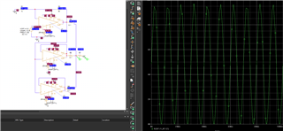
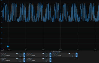
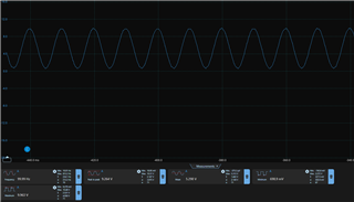
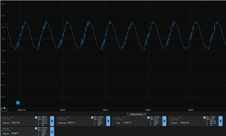
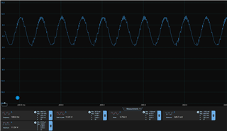
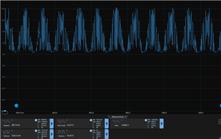
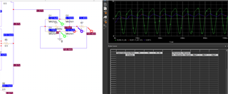
I'm using three OPA549 connected parallelly, one master driving two slave. When 1VAC is applied as non-inverting configuration with gain of 10 getting clean output 10VAC without load. When 1ohm resistive load is applied, when output wave getting noisy. I can see the sine wave but have too much noise.

Note: Below I've already tried, nothing helped.
1) I've tried snubber circuit with different values between 3ohm to 10ohm/ 0.1 uf to 0.01 uf.
2) Very good heat sink
3) Decoulping capacitor both input and output stage
4) RC Filter at output stage

  • Hi Bini Sara,

    I am sorry to hear that you are experiencing troubles in this configuration.

    Do you have any screen captures? This can sometimes give me more clues as for what may be going on. Is this 10VacPk-Pk?

    You have taken the correct approach to debug. Snubbers can be good help for damping inductive or capacitive ringing. Decoupling is very important. RC on output can help knock down some HF noise. 

    Have you tried lighter loads just to see when this large noise starts?

    Do you have a schematic I can look at?

    Thanks,

    Jacob

  • Here I've attached schematics with simulation output waveform. 

    The Snubber and Decoupling I was trying trail and error, So didn't mentioned in the schematics

    In my current setup:
    Snubber circuit value is around 10ohm and 0.1uf at the output stage
    Decoulping cap's value 1000uf at input and 1000uf at the output

    I'll share the real-time waveform in few hours.

  • Yes, the 10VAC is Pk-Pk.Below are the realtime waveform at the output stage in the different scenerio.

    Note: Output Waveform is clean sine wave, With snubber circuit(10ohm/0.1uf) - With Load(6ohm) - Without Decoupling Caps, when starts reducing the load resistance. Noise start to pickup something like below image


    Ouput Waveform: With snubber circuit(10ohm/0.1uf) - Without Load - Without Decoupling Caps


    Ouput Waveform: With snubber circuit(10ohm/0.1uf) - Without Load - With Decoupling Caps at Output Stage(1000uf)


    Output Waveform: With snubber circuit(10ohm/0.1uf) - With Load(1ohm) - With Decoupling Caps at Output Stage(1000uf)


    Output Waveform: With snubber circuit(10ohm/0.1uf) - With Load(1ohm) - Without Decoupling Caps

  • New observation: with 2 OPA549 in parallel in non inverting configuration. with Load 1ohm, with Decoulping Cap at output stage 1000uf and with Snubber circuit 10ohm and 0.1ohm, getting clean sine. But with three why I'm getting noise.

  • These are very helpful to see, thank you for taking the time to take this data. 

    The first waveform does look more like noise than it looks like a sine wave. 

    I tend to trial and error my snubber circuits as well, these values are in a range I would expect to see. 

    The fact that your circuit works with two OPA549's but not three may make me believe we are seeing the amps "fight" one-another. When the devices do not have identical output response, we sometimes the fighting consume more current than the actual output load.

    If you used U1 and U2 for the parallel eval, can you also try U1 and U3 together? Since U1 and U2 match well, one would imagine U1 and U3 should also perform similar. If not, we may have a good place to start making tweaks to the circuit. 

    It may be possible that the ballast resistor needs to be sized up for additional balancing of the different Vos between the devices. 

    I have seen customers use anywhere from .1ohm to even 1ohm depending on the swing to rail needed. I know the DS uses 100mOhm, but it may be possible that the three devices causes enough imbalance to require more resistance. 

    Is the layout between the channels similar? At high currents even relatively small difference can cause issues. 

    It may a good idea to probe the V+ rail close to the DUT pin if you can during this testing. This can be a good way to verify that you have enough decoupling. 

    At the very least, seeing the circuit work with two OPA549's is very promising. 

    What is the minimum load you expect to drive 10Vpk-pk into?

    Thanks,

    Jacob

  • The layout is similar and the 1ohm is the minimum load. I'm planning to increase the ballast resistor to 0.5ohm. Will update once testing is done with it.

    I can also see noise in the V+ rail in the 3 OpAmp configuration and not in the 2 OpAmp configuration

  • Hey Bini,

    Good to hear that the layout is similar.

    Yes, I think 0.5 ohm is a good place to start. 

    This V+ noise may be coming from the oscillation propagating to the V+ rail. It is not uncommon to see that oscillating power amps can cause enough transient current draw to influence the amplitude of the V+ rail. 

    Thanks,

    Jacob

  • Hi Jacob,

    By changing the 0.5ohm now I can able to see clean sine wave. But I'm having the full bridge rectifier circuit after the amplification stage, which affecting the amplification output wave form. 
    I attached simulation images below with explanation. (The simulation image result is same as the real response what I getting in the HW.)


    With no load or 100k as load resistor and 1000u as cap across the rectifier output
    After Amplification stage  10VAC
    After Rectification stage 10DC
    Load Current 0Amp


    With 1ohm as load resistor and 1000u as cap across the rectifier output
    After Amplification stage  10VAC
    After Rectification stage 8AC not getting DC
    Load Current 4Amp(Avg current)


    Increased cap value to make Output DC
    With 1ohm as load resistor and 40000u as cap across the rectifier output
    After Amplification stage  8VAC
    After Rectification stage 6AC(Ripple voltage) not getting DC
    Load Current 6Amp(Avg current)


    After rectification I need 10DC and with 1ohm load. But my amplification output is distorted.

  • Hi Bini,

    Do you mind sending over your Pspice project? I can take a look myself to see if there is anything we can do. 

    Surely some of this is coming from power losses in the rectifier diodes. Some can also be from losses in the Riso resistors. 

    What is the reason for using the rectifier circuit? I assume we are trying to get 10VDC for high current drive. 

    Why not setup the OPA549 to output 10V dc rather than use the rectification circuit to generate the DC voltage?

    Thanks,

    Jacob