This thread has been locked.

If you have a related question, please click the "Ask a related question" button in the top right corner. The newly created question will be automatically linked to this question.

INA333: INA333

Part Number: INA333

Tool/software:

Dear sir,

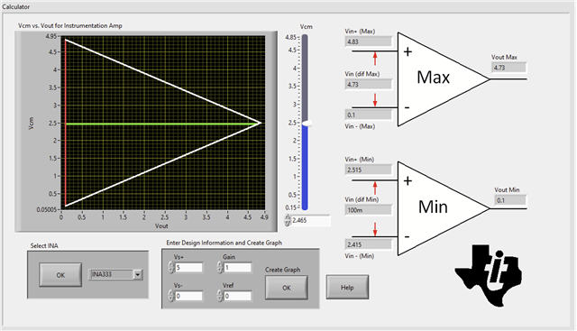
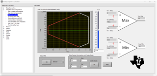
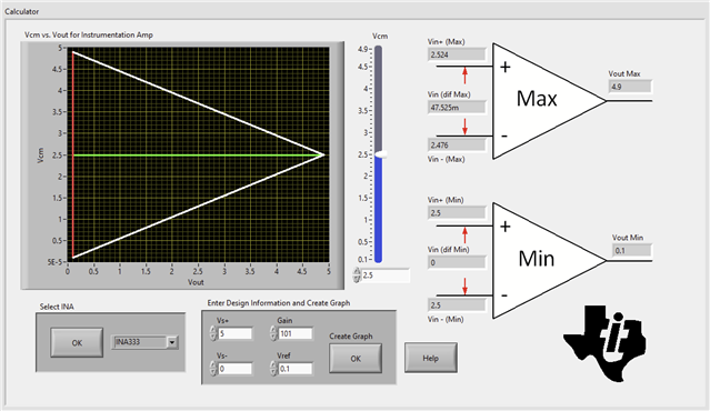
We have configured the INA333 for a single-supply, single-ended input configuration in our custom project. However, we couldn't find any reference to a single-ended input application in the datasheet. Could you please confirm whether a single-ended input configuration is supported by the INA333? Also, if possible, kindly suggest a reference circuit for the INA333 instrumentation amplifier.

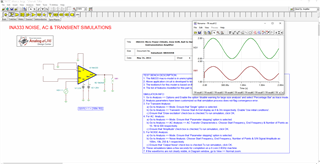
Additionally, we tried simulating the circuit, but it did not work as expected. Please find the attached schematic and simulation report for your reference.

Best Regard,

Samudralankaiah

  • Dear Sir,
    Please find the attached simulation results. The negative peak appears to be clipped. Could you please confirm what might be wrong in the circuit?"

    Best regards,

    Samudralankaiah.

  • Hello Samudralankaiah,

    Please see the Analog Engineer's Calculator to see your valid input common-mode range vs valid output range.

    The ideal transfer function of your device will be ((VIN+ - VIN-)*Gain) + Ref, where gain is 1+ 100k/Rg

    For example, when the input on IN+ is 1V greater than IN- which is at 0, and there is no RG, and Ref is GND, the output will be (1V - 0V)*1 + 0V or 1V. When IN+ is -1V, IN- is still 0, still no RG and Rf is GND. Now the ideal output will be (-1V - 0V)*1 + 0V, the ideal output is -1V. The instrumentation amp cannot output a voltage that is below V-, and therefore will clip.

    Best,
    Gerasimos

  • Dear Sir,

    Thank you very much for your support.

    I would like to confirm the configuration I am planning to use. My input is a single-ended signal from the LT5538 power detector (0 to 2V). The output of the INA333 will interface with the ADC inside the STM32, configured for unity gain.

    The reference voltage is set to mid-supply. The IN– and V– pins are connected to ground, while IN+ is biased at 3.3V.

    The ADC operates within a 0 to 3.3V range, so I believe the output from the INA333 will be well within this limit. Could you please confirm if this configuration is correct and suitable for the intended operation?

    Thank you once again for your guidance.

    Best Regards,

    Samudralankaiah.

  • Hello Samudralankaiah,

    Using the above provided formula ((VIN+ - VIN-)*Gain) + Ref, your range of outputs would be from (0 - 0)*1 + 1.65 or 1.65V, to (2-0)*1 + 1.65 or 3.65V. This exceeds your supply voltage. Additionally, you will be saturating internal nodes inside the amplifier, and you will not even be able to get the 1.65V out. Please download the Analog Engineers Calculator, as this contains the calculator I am using.

    If your inputs are both at 0V, this means your common-mode voltage is 0 and you will have no valid output range.

    Please see the following article on how to interpret VCM vs VOUT Plots: https://www.planetanalog.com/how-instrumentation-amplifier-vcm-vs-vout-plots-change-with-supply-and-reference-voltage/

    If you would like further explanation on how to interpret VCM vs VOUT plots, please let me know.

    Best,
    Gerasimos

  • Hi Sir,
    Thank you for the clarification. I understand now.
    Is it possible to set the Vref to a value lower than the mid-supply, so that we remain within the valid operating range?

    yes I changed to 1.25V. Now I got proper output without clipping. and also within the range.

    Best regards,
    Samudralankaiah

  • Samudralankaiah,

    The effects of varying supply, input voltage, and reference voltage can be seen with the Analog Engineers Calculator: https://www.ti.com/tool/ANALOG-ENGINEER-CALC

    Please let me know if you have any questions on how to use the tool.

    Best,
    Gerasimos