This thread has been locked.

If you have a related question, please click the "Ask a related question" button in the top right corner. The newly created question will be automatically linked to this question.

INA128: IS MY DESIGN WRONG?

Part Number: INA128
Other Parts Discussed in Thread: INA122

Tool/software:

HI,DEAR.

I feel that i will mad because the simplest circuit doesn't work well and i don't konw where is wrong. Can you help me?

Below is my design and J4 is connected to PT100.

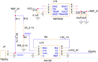
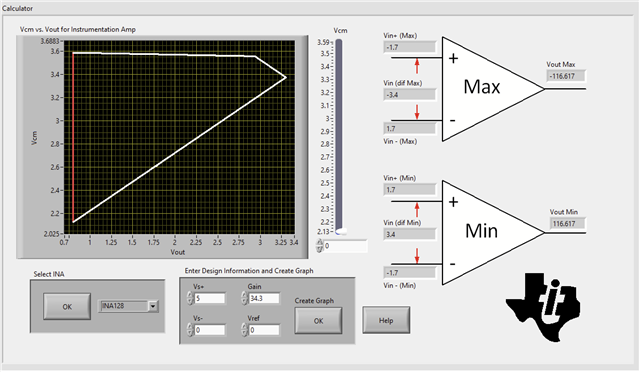
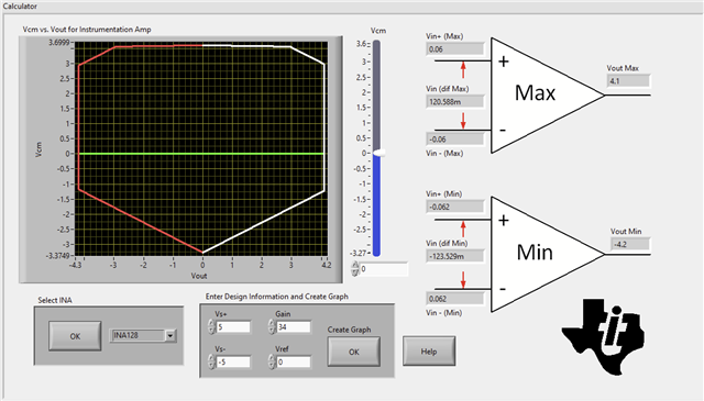
The voltage of Node1 and Node2  is 0.157V and 0.108V seperately. Theoretically the output of the chip pin6 (TEMP2) should be 1.68V. Actually it is only about 0.12V continously.

Thank you!

  • Hello,

    For INA128, in single supply your valid input common-mode range will be 2V from either rail. This means with V+ = 5V, and V- = 0V, valid input common-mode voltage range is 2V to 3V. Your common-mode voltage is (0.157V + 0.108V)/2 = 0.1325V.

    There are multiple ways to fix this:

    1. Decrease your R11/R12 values, however, this will greatly increase the current the REF5030 will need to source. For a common-mode voltage of 2V, R12 and R11 will need to be 112.5 This means your REF5030 will need to source 16mA. This is more than the ref5030 can source, so is not a viable solution.
    2. Choose a different instrumentation amplifier. INA122 is a 2 amp INA with common-mode voltage that includes V-. However, you will need to adjust RG to the correct value for the desired gain. (G34 --> RG = 6.896kOhm)
    3. Add a negative voltage rail for the INA128. Adding a -5V rail to V- of INA128 will make your input common-mode voltage now be in the acceptable voltage range.

    Best,
    Gerasimos