This thread has been locked.

If you have a related question, please click the "Ask a related question" button in the top right corner. The newly created question will be automatically linked to this question.

INA333: INA333

Part Number: INA333
Other Parts Discussed in Thread: TINA-TI

Tool/software:

Hello TI team , 

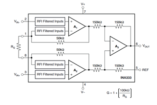
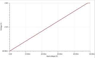
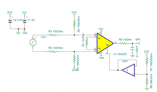
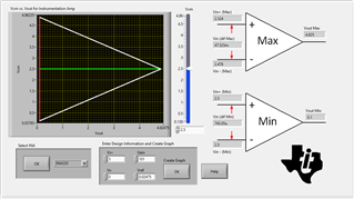
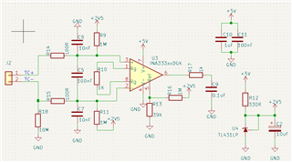
Could you please help to simulate below K thermocouple interface with INA333. We need accuracy ±1%. Temperature range 25'C to 1200C'.

Please look it and revert me asap.

Regards

Jigar Jain

  • Hello Jigar,

    Do you have cold junction compensation? Additionally your current return path R9/R11 may be too large, and there can be noise depending on what impedance is seen by the INA333. The INA333 is a zero-drift amplifier, which has switches on the input that have a charge injection when switched, and this charge injection will cause a voltage spike on the inputs.

    Please see the following article on thermocouple measurements: https://www.ti.com/lit/an/sbaa274a/sbaa274a.pdf

    Additionally, you will not get an accurate output while driving the REF pin with a high impedance source. You need a low-impedance reference voltage, like a buffered op amp, to drive the REF pin, as whatever impedance is seen on the REF pin will result in gain error on the output. Looking at the schematic of the device, the impedance seen on REF will add in series with the 150kOhm resistor, and the gain will now be greater than one between the output of A2 and Vout.

    We cannot run simulations to verify performance of 1% accuracy, we can only run simulations to confirm the function of the circuit. The SPICE models we provide are macromodel approximations of the function of the device.

    You may evaluate the circuit in either one of our simulators

    https://www.ti.com/tool/TINA-TI

    https://www.ti.com/tool/PSPICE-FOR-TI

    Best,
    Gerasimos

  • Hello Gerasimos,

    Thanks for the feedback. Yes, we have the cold junction compensation.

    Regarding R9/R11, please advise on the R9/R11 value for a better solution.

    Regarding the REF pin, We will use an additional buffer op-amp as suggested. 

    Regarding simulation, Just simulate the design and let me know if require changes. Accuracy we will check.

    Again, thanks for the quick response. I appreciate your further support. 

    Regards

    Jigar Jain

  • Jigar,

    Here is the simulation file and results

    INA333_JIGAR.TSC

    Note that the VCM vs VOUT is not modeled correctly, and will need to be evaluated using the Analog Engineer's Calculator.

    With the parameters provided, your minimum input differential that will be linear amplified is 745uV, and the maximum differential voltage for linear amplification will be 47.525mV

    Best,
    Gerasimos

  • Hi Gerasimos,

    I checked practically and find that design working well. But i dont understand why this is not working in simulation model ? 

    Or Simulation tool is not working as we understand. Could you please look it here and provide further solution. 

  • Hi Jigar,

    But i dont understand why this is not working in simulation model ?

    When you say simulation model, you mean TINA-TI / PSpice simulation? 

    These models are not designed for replicating the common mode vs output voltage plot. This is one of the reasons why we have the Analog Engineer's Calculator 

    In simulation of analog circuits, there is a phrase often used: "Trust but verify" E2E Link

    These macromodels are designed to emulate performance of the device in the most common use-cases. Most INA models do not perfectly represent the VCM vs. Vout plot as the macromodel is supposed to be a blend between accurate performance and short convergence time. Please consider using the Analog Engineer's Calculator for verifying performance limits over common mode setting. 

    Best,

    Jacob