Other Parts Discussed in Thread: ADS1299, INA350, TINA-TI, OPA350
Tool/software:
Hi,
I'm really a software developer and not good at electronics, so please bear with me.
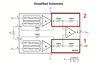
I was recommended the INA333 as a pre-amp for reading EEG, and bought the following module to have a play with it before potentially using a more complex/custom board design
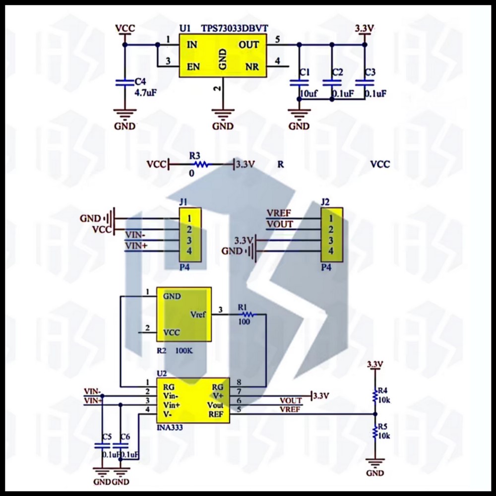
Currently I do not seem to be getting the sort of noisefloor I was hoping for; I think the layout of the board makes sense to me, but in particular I note from the datasheet that:
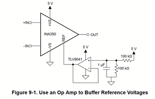
> 8.2 Typical Application
> The output of the INA333 device is referred to the output reference (REF) pin, which is normally grounded. This connection must be low-impedance to assure good common-mode rejection. Although 15 Ω or less of stray resistance can be tolerated while maintaining specified CMRR, small stray resistances of tens of Ωs in series with the REF pin can cause noticeable degradation in CMRR.
Right now I am considering single-channel only, so the inputs are a true differential pair between two electrodes, one as the reference.
The board provides a single supply voltage, so I understand the reason for fixing the reference output halfway between +3.3V and ground with R4 and R5, and therefore that using low-value resistors here would draw an enormous amount of current from the positive rail. However, given that the datasheet explicitly mentions the importance of having a low-impedance path to ground for the reference pin, I am wondering, is this an error on the part of the designers of the board? Or is there a reason why it would be expected and a valid thing to have something as high as 10kΩ in this configuration?
I have tried putting a small resistor between the reference and ground, and not seen much improvement in the noise levels, although that may be an issue elsewhere, especially whilst I am prototyping and the noise all the way through will be somewhat high.
Would anyone have an opinion on the design of this board at all please?
Thanks a lot