Tool/software:
Hello,
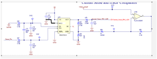
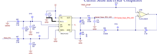
Please find the below schematic of INA241A2.
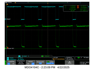
During testing , 115mV of signal was fed across IN- and IN+ at TP15 and TP17 points.
With 80% input duty cycle , we are observing output voltage reaches 2.120V where input voltage is 0.115mV (Ideally output had to be 0.115*20 which is 2.3V).
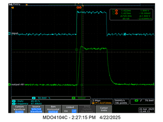
But with 20% input duty cycle , we are observing output voltage reaches 1.89V where input voltage is 0.115mV (Ideally output had to be 0.115*20 which is 2.3V)
Could you please explain why Gain is varying wrt input duty cycle and there is a lot of error in Gain.