This thread has been locked.

If you have a related question, please click the "Ask a related question" button in the top right corner. The newly created question will be automatically linked to this question.

LMH6554: Technical Inquiry about LMH6554

Part Number: LMH6554
Other Parts Discussed in Thread: ADS4249

Tool/software:

Dear Engineer:

        Please help us to confirm the following 3 issues:

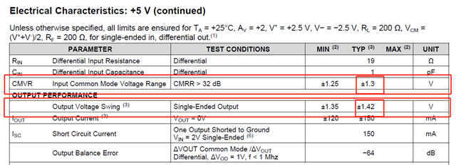
        Issue 1:In the LMH6554 datasheet(SNOSB30P –OCTOBER 2008–REVISED JANUARY 2015),the CMVR is ±1.3V,the Output Voltage Swing is ±1.42v,I want to konw what  is the voltage(±1.3V  ±1.42V) refered to? refer to GND or (V+ + V-)/2 ? 

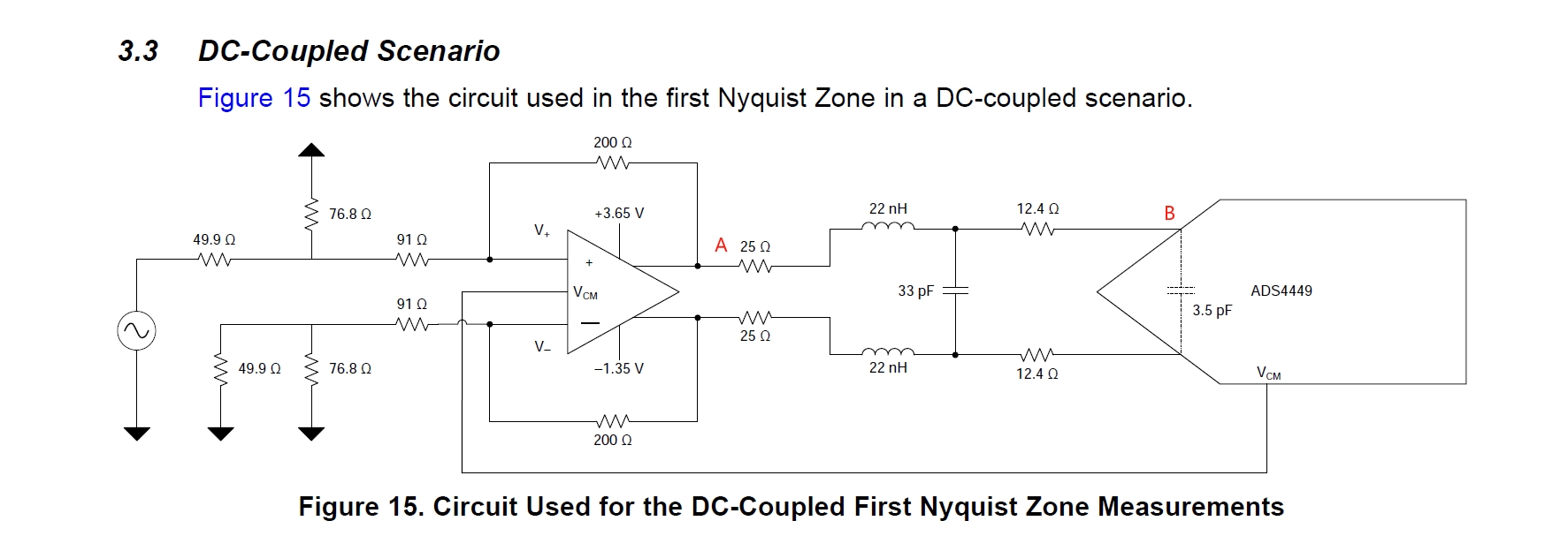
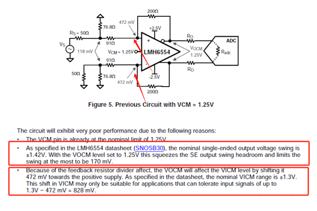
        Issue 2:In the document 《AN-2177 Using the LMH6554 as an ADC Driver》,the VICM is adjusted to 1.25V,the normal VICM range is ±1.3V in the LMH6554 datasheet,this make the device can only tolerate the signals up to 1.3V-1.25V=50mv。The output voltage swing is  ±1.42V,the SE output swing remain 170mV。What's the purpose of adjusting the VICM to 1.25V via  pull-up resistors?

  Issue3:What is the specified voltage range for the output common-mode voltage(the voltage on the Vcm pin)?

  • Hi,

    Issue1:  The CMVR and output swing voltage (±1.3V and  ±1.42V respectively) refer to mid supply voltage [(V+ + V-)/2 ]

    Issue2: You can refer to the paragraph following the Figure 5 (Page 5) of  the document 《AN-2177 Using the LMH6554 as an ADC Driver. It explains the purpose of adjusting the VICM to 1.25V via  pull-up resistors

    Issue3: The output common mode voltage range is ±1.25V. It is given in Page 6 of the datasheet

    Regards

    Anant 

  • Hi

            In the 《AN-2177 Using the LMH6554 as an ADC Driver》,We can't download the Design Zip File,Can you sent me the Design Zip File.

            Best Regards

            Aaron

  • Hi Aaron,

    Let me look at this issue of broken link in the pdf.

    I will provide you the Design file by early next week.

    Regards

    Anant

  • Hi,

             We use the LMH6554 to drive the ADC as Figure 1,the ADC is ADS4249.The LMH6554 converts the 10 MHz(1V VPP) single-ended signal into a differential signal and outputs it to the ADS4249.The sampling frequency of the ADS4249 is 250 MHz.When we used an oscilloscope to measure the waveform at point B, we observed a 250 MHz high-frequency signal superimposed on the 10 MHz output signal as Figure 2.When measuring point A with an oscilloscope, this phenomenon was not observed.When the 22nH inductor is replaced with a 0-ohm resistor, this phenomenon also disappears.The 250 MHz high-frequency signal appears to be related to the ADC sampling and the 22nH inductor.How much does this 250 MHz high-frequency signal affect the ADC sampling accuracy, and can we replace the 22nH inductor with a 0-ohm resistor?

                                                                            Figure 1

                                                                      Figue 2

  • I am looking at this, will get back to you on this bytomorrow

  • Hi,Anant

            Thank you very much.Please help us to analyze this issue, and send us the link of the design documents.

            Best Regards

    Aaron


  • Hi Aaron,

    Sorry for delay in response.

    You can remove inductor but you need ensure that the proper cutoff for the anti aliasing filter and charge bucket filter is selected.This can be achieved using just the R and C also. 

    There are few training videos which explains how the filter value is selected based on the sampling rate the and signal bandwidth. Attaching the link below:-

    https://www.ti.com/video/series/precision-labs/ti-precision-labs-analog-to-digital-converters-adcs.html#

    Below are the section which I recommend you to go through

    1>  AC and DC Specifications> Aliasing and anti-aliasing filters

    2> SAR ADC Input Driver design

    Regarding the design file in the borken link of the document, please give us few more days to fix the issue.

    Regards

    Anant

  • Hi,Anant          

            Is  ADS4249 the SAR ADC or Delta-Sigma ADC?How can I convert the LVDS output into actual voltage signals? For example, if the ADC samples a 1V input signal, what digital signal should the LVDS output?

            Regards

            Aaron

  • Hi Anant

            Can you send me the design file by e-mail before you fix the  borken link issue,We need to complete the PCB modifications next week.

            Regards

            Aaron

  • ADS4249 is a SAR ADC, I will assign this thread to ADC team who can help you better on this query regarding the ADC questions.

  • Closing this post, this ADC question was answered on this E2E post: e2e.ti.com/.../5850360