This thread has been locked.

If you have a related question, please click the "Ask a related question" button in the top right corner. The newly created question will be automatically linked to this question.

INA592: use in G=2 mode

Part Number: INA592
Other Parts Discussed in Thread: INA597, STRIKE

Tool/software:

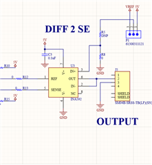
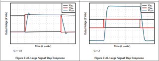
I'm trying to use this part in the G=2 mode, datasheet states this is possible. I have the -IN connected to OUT and the source negative input goes to SENSE, and the source positive input goes to REF and +IN goes to GND. Operating off +5V & GND. Only seeing 0V at OUT. The datasheet implies this mode is possible, but can it actually work this way? Am I missing something?

  • Hey Mark,

    This certainly is possible!

    What input voltages are you providing on SENSE and REF?

    Best,
    Gerasimos

  • +4.5V on REF and +0.5V on SENSE. I realize this will rail the output, but I'm measuring 0V on OUT. I have other upstream problems, but need to make sure this is working first. 

  • Hey Mark,

    Correct, this should be railing the output, but to the positive rail (about 130mV below V+).

    Do you have a picture of your connections? How are you setting up this circuit (PCB, breadboard, something in between?)

    Best,
    Gerasimos

  • PCB implementation, pretty straightforward design. Could definitely just be a blown part, but wanted to make sure design was correct first.

  • The connections do look correct!

    I do have some comments for some general improvements that are probably unrelated to your output low issue.

    1. Since the output is going to an off-board connector, be mindful of the capacitive load drive of the amplifier. In general, it can be helpful to populate a 0ohm resistor in series with the output, in case isolation resistance is needed.
    2. This footprint will also help my second point, of ESD protection. If this is a user accessible connector, it may be helpful to add ESD diodes between the isolation resistor and the connector, to mitigate potential ESD damage to the amplifier.

    Let me know if you do determine this to be a damaged device.

    Best,
    Gerasimos

  • Hi Gerasimos,

    It did turn out to be a damaged device, but now the output appears to run opposite of the expectation. Any chance the REF & SENSE pins are incorrect in the datasheet? I know that is unlikely, but this one is a head-scratcher.

    Mark

  • Hey Mark,

    I haven't heard anything like that happening, however, this can be tested with a multimeter.

    If you measure impedance between IN+ and REF, and IN+ and Sense, the resistance between IN+ and REF should be roughly the sum of the 12k and 6k resistors, and the other should be much higher, as that node passes through the high impedance of the base of the input transistor (or some lesser impedance parasitic path).

    By opposite of the expectation, are you expecting an increase in REF to increase relative to SENSE to increase your output voltage, and an increase in SENSE relative to REF to decrease your output voltage?

    Best,
    Gerasimos

  • Hey Gerasimos,

    Using a DMM on the INA592 in circuit, measuring +IN to REF I get 10K in both polarities. Measuring -IN to SENSE I get 10K, and SENSE to -IN is get 18K, but -IN is also tied to OUT which might explain it. This isn't what I was expecting at all.

    The reason I think there is an issue is this: I have a negative differential REF to SENSE of -0.2V, yet the output is +2.9V. With the negative differential I was expecting +2.1V. Thoughts?

    Mark

  • Hey Mark,

    A couple thoughts:

    1. Those impedance values correspond with what is expected per the datasheet.
    2. In a gain of two, the output should be 0.4V if the input differential is a -0.2V between REF and SENSE. What is the common-mode of this input signal?
    3. Impedance on the resistor to ground can introduce gain error and disrupt CMRR, however, it usually will not be to the order of hundreds of mV.
    4. Is it possible there is a floating ground plane or ground island? Is the potential at the local ground the same as the source ground?

    Best,
    Gerasimos

  • Hey Gerasimos,

    1) OK.

    2) My comments above were in general, so I remeasured these just now: REF=1.410V, SENSE=1.572V, diff then is 0.162V, OUT=2.901V. Isn't the output biased up to Vs/2 = +5.0/2 = +2.5V in this case? Section 7.6 of the datasheet implies that.

    3) OK.

    4) Someone else laid this out, but this is a test board and only a 2-sided PCB. Looking at the layout all is interconnected properly.

    Mark

  • Sorry, in 2) above the diff is -0.162V.

  • Hey Mark,

    Is there a voltage on IN+ biasing up to 2.5V? Per the schematic you linked there is a 0ohm to GND, and a jumper that allows for connections to different potentials.

    Assuming there is a 2.5V ref, your output should be 0.162V*2+2.5. This means that the expected output voltage is 2.824V. However, if your gain was supposed to be 2, and you are seeing a gain error of +23%, my first thought is to check the impedance of what is supplying your reference voltage on IN+.

    If there is a mid-supply potential connected to a voltage reference to create the 2.5V, or is this fed from a voltage divider? If this is fed from a voltage reference and there is not much impedance between the reference and IN+, then our issue is elsewhere. However, if this is fed from a voltage divider, this will cause significant gain error.

    Best,
    Gerasimos

  • Hey Gerasimos,

    There is no voltage on +IN, the resistor to the header in DNP (Do Not Populate). 

    My read of the datasheet says there should be an embeeded Vs/2 common voltage on the output? I thought that was what I was seeing on the output.

    My apologies in advance... I'm trying to troubleshoot thos PCB without major surgery - it's needed to support testing, and with 0402 resistors it's not easy to play with... but I may be at that point...

    Mark

  • Hey Mark,

    That information is the provided test conditions for the stated measured electrical characteristics. The input common mode and output common mode are being driven to V+/2. In split supply, this means that the input CM and output CM are both GND. This is just providing a reference point to start adding other errors on top of, and does not mean that the output is natively driven to midsupply.

    For example, if you were measuring input offset voltage with your output centered on 0V, but your common mode was 2V, you would have to take the input offset voltage, plus the error contribution from CMRR (2V/ 94dB) similarly for output voltage, if your input CM was now 0V, and your output was biased to 1V, then your error will be the combined error of the gain error seen from your reference to out combined with your AOL error. Since AOL is typically very large, the gain error term will dominate.

    However, the transfer function of this circuit will be

    VOUT = (VREF - VSENSE)*2 + VIN+

    In this case, if the voltage at IN+ is GND, your output voltage should be just the 324mV.

    Best,
    Gerasimos

  • Hey Gerasimos,

    Thanks for your quick reply. I guess I misread the datasheet. But the problems persist...

    I removed the input zero ohm resistors (R12 & R13 above) and here's what I found: REF = +2.353V, SENSE = +2.992V, OUT = +2.996V. Grounding either input droped OUT to ~2.9V.

    So my question now is: Has anyone ever used this part in G=2 mode? Can someone on your end try my simple circuit above and see what they get? No resistors are necessory - tell me if they get a diff gain of 2. Can this be done?

    Mark

  • Hey Mark,

    The device has been qualified and has measured data in G1/2 and G2. The typical characteristic plots are measured data from real silicon in both configurations.

    Floating the inputs will cause the bias current to charge the inputs to a max value, and it will not operate linearly. What is supplying your input voltage? Are you supplying directly from a benchtop supply?

    Best,
    Gerasimos

  • Hey Gerasimos,

    In the final application the inputs will be driven by a diff in/diff out VGA (AD8338). But right now the inputs are floating and when I ground them the output is ~+2.9V, which doesn't make sense.

    I was lured in with the e-trim technology to achieve good differential-to-SE processing, but is this the correct part for thsi application? What is the difference between the INA592 and INA597, just just offset and offset drift? Any other self-contained items you offer vs. an op amp and 4 resistors?

    Mark

  • Hey Mark,

    This device is a good fit for a differential to SE processing. Difference amplifiers work well here. If you were looking for a single chip DE-to-SE conversion, this type of device is what I would recommend.

    The differences between the INA592 and INA597 are the offset voltage and drift performance, yes. One has a tighter trim than the other.

    The proper way to test this circuit would be to do the following:

    1. Ensure the supply voltages are correctly 5V on V+ and 0V on V-
    2. Ensure IN+ is driven to 2.5V with a low-impedance source (not from a resistor divider)
    3. Supply REF and SENSE with 2.5V from a low-impedance source (you can reuse the 2.5V supplied to IN+)
    4. Measure the output. The output should be 2.5V, plus the offset voltage of the amplifier (10s of uV)
    5. Now from this voltage, vary REF. Increasing REF above 2.5V should cause the output to increase by twice the amount increased, decreasing REF below 2.5V should cause the output voltage to decrease by twice the amount decreased

    Best,
    Gerasimos

  • Hey Gerasimos,

    The input differential voltage should not swing negative in normal operation (despite the negative differential listed above, that was due to a schematic error reversing pos and neg earlier in the signal chain than I have to fix, but the AD8338 is powered by a single voltage and adds offset anyway). So I should not have to add +2.5V to this circuit as you indicated in 2) above - the resistor divider on +IN was just in case low differential values were occuring to get it off the lower rail. So shouldn't I be able to run the circuit as I've shown above? I still don't see why I'm getting +2.9V for grounded inputs on REF and SENSE. Shouldn't I be getting 0V on OUT?

    Mark

  • Hey Mark,

    If both inputs are grounded, and the IN+ pin (your voltage reference) is 0V, your output should ideally be 0V, but in reality it will be V- + the negative swing from rail of the device. In this case it is roughly 190mV. If your output is 2.9V, there are only a couple possible things that could cause this, since this is not a value near the extremes of the output voltage range (V+ or V-)

    1. GND is not actually 0V, and the V- pin is actually ~2.9V (probably closer to 2.7V due to swing limitation)
    2. There is a voltage present on IN+ (reference voltage) and it is forcing the output voltage up. It would have to be roughly 2.9V if the inputs are both 0V.
    3. The inputs (REF and SENSE) are not both properly driven to 0V, IN+ is properly being driven to 0V, and there is actually a 1.45V difference between the two inputs
    4. Something is loading the output and pulling the output voltage to be 2.9V. (for the output to be pulled to 2.9V, it would have to be loading the output with ~40mA of current.
    5. There is an excessively large capacitive load on the output of the device, it is unstable, and the DMM is averaging this value and seeing it as 2.9V.

    There may be a few other cases, but these are the most common ones I could think of.

    The steps I listed in my previous answer were how to test the device independently of other devices in the system to ensure correct operation of the device.

    Are you able to provide the schematic of what is connected to the other end of the connector (J5)?

    Best,
    Gerasimos

  • Hey Gerasimos,

    This is not my first rodeo... I've checked many of the things you listed already without mentioning them, but checked them again for completeness:

    1) GND is GND, measures zero volts, confirmed a short to the power connections were the return is applied. It's a simple 2-layer PCB we made for testing purposes for the analog chain.

    2) There is no voltage present on IN+ WRT to GND.

    3) I soldered a wire across the pins (the side of R12 & R13 to REF & SENSE) and tied it to GND. OUT is still +2.9V.

    4) There is nothing loading OUT, there is nothing connected to J5. It would eventually go to an ADC but it is not needed for this troubleshooting.

    5) There is no capacitance on OUT. I had not been looking at OUT with a scope since the DMM was rock solid - I have since looked at it with a scope and there is no oscillations present - it is a DC level. I even checked if the device was mounted properly, and the pin 1 marks align.

    This is not the first time in my career where I've defied the laws of physics, but I have mounting pressure to get this moving. Any other thoughts on this besides this being another bad part? If blown, it's odd to be at +2.9V. Let me know your thoughts. Thanks.

    Mark

  • Hey Mark,

    I definitely didn't want to doubt your experience, and to be similarly thorough on my end, I soldered up an EVM and tested with the following conditions, and got the expected results.

    Pin1: Non-inverting input
    Pin2: connected to Pin6
    Pin3: GND
    Pin4: GND
    Pin5: Inverting input
    Pin6: connected to pin2, output voltage measured here
    Pin7: 5V
    Pin8: No connect

    When shorting both inputs (pin 1 and 5) to GND together, the output voltage was in the single digit mV range.

    When driving the noninverting (pin 1) input to 100mV, I was seeing the correct 200mV on the output. As I swept the input, I saw the correct corresponding output voltage on pin 6. I have triple-checked the connections above.

    Is there something that is likely damaging these devices? I agree that it would be atypical to be damaged and near midsupply on the output, that's not something I have usually seen.

    Best,
    Gerasimos

  • Hey Gerasimos,

    My apologies if I seemed to huffy - I just wanted it to be clear you weren't deling with a neophyte. When this problem became defiant of the laws of physics, I knew I needed help - thanks for your patience. This message will only serve as a status...

    I fear we got a bad lot of parts - we are hand assembling the PCBs with proper protocols, but after two failures I have my doubts about the quality of parts we received. That said, I ordered and received more parts, plus some OTS SSOP adapter boards (link below) to solder up and try things out. Since there are no components needed for this circuit, I just need to add wires. I'll let you know what I find out. Stay tuned...

    Mark

    https://www.digikey.com/en/products/detail/sparkfun-electronics/00497/5318735?s=N4IgTCBcDaKHAEBGArANgBwFoAMWAsBOAdgwDkAROEAXQF8g

  • Hey Mark,

    No worries at all! I was hoping I didn't offend. When things seem to be defying logic, I try to take a step back and recheck any and all assumptions, including things as simple as board power.

    Are you ordering the parts from the TI store or from an authorized distributor? If so, they should have been handled properly and arrive working.

    Best,
    Gerasimos

  • Hey Gerasimos,

    The TI parts I got were from Digi-Key, we've had good luck with them before. Similar to you I built up a small test board in my configuration, and as expected it works as designed. Possible reasons for not working on our main board:

    1) ESD strike during soldering
    2) Transient overvoltage in main board smoking it.
    3) We got a bad batch of parts initially.

    I have issues with other parts on this design, so I plan to move to them next - some are TI parts, so maybe we'll speak again in another thread... LOL! But I just wanted to thank you for putting in the time to help me with this - I wanted to make sure I wasn't losing my mind...

    Mark

  • Hey Mark,

    Happy to help! If you do have any questions in the future feel free to reach out! I answer questions on difference amplifiers and instrumentation amps, so if you have more questions with those, it is likely going to be me or my colleague Ashley! Otherwise you'll land with one of the many other qualified experts at TI.

    I'm going to mark this thread closed.

    Best of luck!
    Gerasimos